
カタログの抜粋
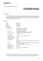
Ultra low power Audio Decoder LSI The CXD5091AGG is an audio decoder LSI that achieves super-low power consumption and supports many codecs. Useful interface such as NAND/NOR flash memory and Memory Stick is supported, and it comprises analog circuits such as audio D/A converter and SAR A/D converter. The CXD5091 AGG is suitable for portable audio players and cellular phone audio backend. NAND flash interface Serial interface Clocked serial interface Memory Stick interface Audio interface Watchdog timer SRAM, NOR flash slave compatible Host processor can be connected. An external acknowledge device is also supported. 4-symbol ECC, Reed-Solomon error correction X 2ch (1ch supports up to 3Mbps baud rate.) Either analog audio interface or l2S bus interface can be selected as transfer PHY included, Low/Full/High-speed device, 5 end points, Control/Interrupt/ Bulk/Isochronous transfer X 8ch, internal clock/external event trigger Sony reserves the right to change products and specifications without prior notice. This information does not convey any license by any implication or otherwise under any patents or other right. Application circuits shown, if any, are typical examples illustrating the operation of the devices. Sony cannot assume responsibility for any problems arising out of the use of these circuits.
カタログの1ページ目を開く
Sampling rate converter ♦ Signal processing accelerator: Virtual Mobile Engine 8 to 96kHz sampling frequency is converted to 44.1 kHz. Peak detection 116 (When all multiplexed pins are setas GPIO), Direction individually selected 45.1584MHz input, Crystal/Ceramic selectable 12MHz input, Crystal/Ceramic selectable In this data sheet abbreviations shown below are used to simplify descriptions.
カタログの2ページ目を開く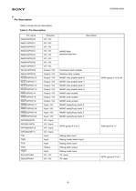
CXD5091AGG Pin Description Table 2 shows the pin description. Table 2. Pin Description Pin name Direction Description NAD0/GPIOC0 I/O / I/O NAD1/GPIOC1 I/O / I/O NAD2/GPIOC2 I/O / I/O NAD3/GPIOC3 I/O / I/O NAD4/GPIOC4 I/O / I/O NAD5/GPIOC5 I/O / I/O NAD6/GPIOC6 I/O / I/O NAD7/GPIOC7 I/O / I/O NCLE/GPIOC8 Output / I/O Command latch enable NALE/GPIOC9 Output / I/O Address latch enable NCE0/GPIOC10 Output / I/O NAND chip enable bank 0 NCE1/GPIOC11 Output / I/O NAND chip enable bank 1 NCE2/GPIOC12 Output / I/O NAND chip enable bank 2 NCE3/GPIOC13 Output / I/O NAND chip enable bank 3 NRE/GPIOC14...
カタログの8ページ目を開く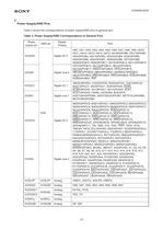
Power Supply/GND Pins Table 3 shows the correspondence of power supply/GND pins to general pins. Table 3. Power Supply/GND Correspondence to General Pins VREFL, AOUTL, AOUTR, VREFR
カタログの15ページ目を開く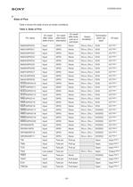
Table 4 shows the state of pins at certain conditions. Table 4. State of Pins
カタログの16ページ目を開く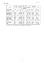
n For Dlom, DI0L1, DI0H2 and DI0L2, refer to Table 7 Electrical Characteristics.
カタログの21ページ目を開く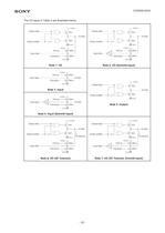
The I/O types in Table 4 are illustrated below. Output data Output enable Input data Output data Output enable Input data- Note 2. I/O (Schmitt Input) Input data Input data-<OÎL Output data Note 4. Input (Schmitt Input) Input data-"CXi. Note 7. I/O (5V Tolerant, Schmitt Input)
カタログの22ページ目を開く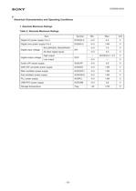
Electrical Characteristics and Operating Conditions 1. Absolute Maximum Ratings Table 5. Absolute Maximum Ratings
カタログの23ページ目を開く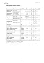
2. Recommended Operating Conditions Table 6. Recommended Operating Conditions n Refer to I/O Type column in Table 4 State of Pins. *2 Offset for DVDKO-2 shall be less than 0.3V. *3 When SCL/GPIOKO and SDA/GPIOK1 are in use, the minimum voltage must be as low as 1.8V.
カタログの24ページ目を開く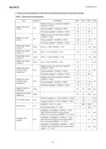
3. Electrical Characteristics Under Recommended Operating Temperature Range Table 7. Electrical Characteristics
カタログの25ページ目を開く
n Refer to GPIO setting in user's manual. *2 Refer to Output Drivability column in Table 4 State of Pins. *3 Refer to Output Drivability column in Table 4 State of Pins. *4 Ceramic mode: For OSC45, keep MCSEL pin "H". For OSC12, set SCSEL bit to "1 " in SCLE register *5 Crystal mode: For OSC45, keep MCSEL pin "L". For OSC12, set SCSEL bit to "0" in SCLE register *6 Set SPLLEN bit to "1 ", set SFDEV1 bit to "0", and set SFDEV0 bit to "1 " in SCLE register (3000001 Oh). *7 Set SOSC bit to "1 " in CLC register (30000000h) and set SPLLEN bit to "0" in SCLE register (3000001 Oh), then set to...
カタログの26ページ目を開く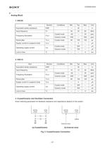
Analog Block 3. Crystal/Ceramic and Oscillator Connection Exact matching parameters for feedback resistance and capacitance depend on the system. (a) Crystal/Ceramic (b) External clock
カタログの27ページ目を開く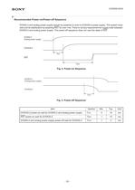
Recommended Power-on/Power-off Sequence DVDKO-2 and analog power supply should be powered on prior to DVDIOO-2 power supply. The system must wait until its stabilization by asserting RST for over 1 ms. There is not any requirement for supply order between DVDKO-2 and analog power supply. The power-off sequence does not care the state of RST. Analog power supply Analog power supply
カタログの30ページ目を開く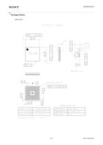
Package Outline PACKAGE STRUCTURE Sony Corporation
カタログの31ページ目を開くSony Semiconductors/ソニーのすべてのカタログと技術パンフレット
-
 IMX901-AMR
2 ページ
-
 IMX490
2 ページ
-
 IMX290NQV
2 ページ
-
 ISX016
2 ページ
-
 IMX390CQV
2 ページ
カタログアーカイブ
-
 IMX249LLJ/IMX249LQJ
2 ページ
-
 IMX183CLK-J/CQJ-J
2 ページ
-
 IMX273LLR/LQR
2 ページ
-
 IMX253LLR/LQR
2 ページ
-
 IMX294CJK
2 ページ
-
 IMX385LQR
2 ページ
-
 IMX324
2 ページ
-
 IMX412-AACK
2 ページ
-
 IMX367LLA
2 ページ
-
 IMX222LQJ
2 ページ
-
 IMX302LQJ
2 ページ
-
 IMX258
2 ページ
-
 IMX323LQN
2 ページ
-
 IMX249LLJ/LQJ
2 ページ
-
 IMX377CQT
5 ページ
-
 IMX230
2 ページ
-
 IMX252LLR/LQR
2 ページ
-
 IMX291LQR
2 ページ
-
 CXG1407XR
11 ページ
-
 SLD332F
6 ページ
-
 CXA3791EN
13 ページ
-
 ICX642BKA
23 ページ
-
 ICX418ALB
20 ページ
-
 CXM3569XR
13 ページ
-
 CXM3570ER
13 ページ
-
 CXM3572ER
14 ページ
-
 CXM3580AUR
17 ページ
-
 CXM3580UR
13 ページ
-
 CXM3582UR
17 ページ
-
 CXM3583AUR
17 ページ
-
 CXM3592AUR
15 ページ
-
 CXM3593UR
11 ページ
-
 CXM3599UR
15 ページ
-
 CXM3604UR
14 ページ
-
 CXM3614ER
14 ページ
-
 CXM3617ER
23 ページ
-
 CXM3630UR
15 ページ
-
 CXM3632ER
22 ページ
-
 CXM3641ER
22 ページ
-
 CXM3642K
29 ページ
-
 CXM3645ER
12 ページ
-
 CXM3648UR
11 ページ
-
 CXM3807K
24 ページ
-
 CXA2984GC SP4T ANT SW
11 ページ
-
 CXA4416GC
21 ページ
-
 SLD433S4
5 ページ
-
 CXA2096N
17 ページ
-
 ICX205AK
24 ページ
-
 CXB1818Q
17 ページ
-
 CXA3314ER
16 ページ
-
 SLD432S
5 ページ
-
 SLD344YT
6 ページ
-
 SLD335YT
5 ページ
-
 SLD1332V
5 ページ
-
 CXD4728R
68 ページ
-
 CXD4017R
34 ページ
-
 CXA3197R
30 ページ


