
カタログの抜粋

Desktop 3rd Generation Intel® Core™ Processor Family, Desktop Intel® Pentium® Processor Family, and Desktop Intel® Celeron® Processor Family Datasheet – Volume 2 of 2
カタログの1ページ目を開く
INFORMATION IN THIS DOCUMENT IS PROVIDED IN CONNECTION WITH INTEL PRODUCTS. NO LICENSE, EXPRESS OR IMPLIED, BY ESTOPPEL OR OTHERWISE, TO ANY INTELLECTUAL PROPERTY RIGHTS IS GRANTED BY THIS DOCUMENT. EXCEPT AS PROVIDED IN INTEL'S TERMS AND CONDITIONS OF SALE FOR SUCH PRODUCTS, INTEL ASSUMES NO LIABILITY WHATSOEVER AND INTEL DISCLAIMS ANY EXPRESS OR IMPLIED WARRANTY, RELATING TO SALE AND/OR USE OF INTEL PRODUCTS INCLUDING LIABILITY OR WARRANTIES RELATING TO FITNESS FOR A PARTICULAR PURPOSE, MERCHANTABILITY, OR INFRINGEMENT OF ANY PATENT, COPYRIGHT OR OTHER INTELLECTUAL PROPERTY RIGHT. A...
カタログの2ページ目を開く
Revision History Revision Number Revision Date Initial release Updated Section 2.6 to reflect support for Functions 0–2. Updated Section 2.7 to relfect support for Functions 0–2. Added Desktop Intel® Pentium® processor family support Added Desktop Intel® Celeron® processor family support Updated Section 2.6.49, “LCTL2—Link Control 2 Register” Added Section 2.10.45, RSTS—Root Status Register Added Section 2.10.46, DCAP2—Device Capabilities 2 Register Added Section 2.10.47, DCTL2—Device Control 2 Register Added Section 2.10.49, LCTL2—Link Control 2 Register Added Section 2.10.50, LSTS2—Link...
カタログの11ページ目を開く
Introduction This is Volume 2 of the Datasheet for the following products: • Desktop 3rd Generation Intel® Core™ processor family • Desktop Intel® Pentium® processor family • Desktop Intel® Celeron® processor family The processor contains one or more PCI devices within a single physical component. The configuration registers for these devices are mapped as devices residing on the PCI Bus assigned for the processor socket. This document describes the configuration space registers or device-specific control and status registers (CSRs) only. This document does NOT include Model Specific...
カタログの12ページ目を開く
Processor Configuration Registers Processor Configuration Registers This chapter contains the following: • Register terminology • PCI Devices and Functions on processor • System address map • Processor register introduction • Detailed register bit descriptions Register Terminology Table 2-1 lists the register-related terminology and access attributes that are used in this document. Table 2-2 provides the attribute modifiers. Register Attributes and Terminology Item Read Only: These bits can only be read by software, writes have no effect. The value of the bits is determined by the hardware...
カタログの13ページ目を開く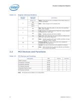
Processor Configuration Registers Register Attribute Modifiers Attribute Modifier Description Sticky: These bits are only re-initialized to their Reset Value by a "Power Good Reset". Note: Does not apply to RO (constant) bits. Key: These bits control the ability to write other bits (identified with a 'Lock' modifier) Lock: Hardware can make these bits "Read Only" using a separate configuration bit or other logic. Note: Mutually exclusive with 'Once' modifier. Once: After reset, these bits can only be written by software once, after which they become "Read Only". Firmware Write: The value of...
カタログの14ページ目を開く
Processor Configuration Registers System Address Map The processor supports 512 GB (39 bit) of addressable memory space and 64 KB+3 of addressable I/O space. This section focuses on how the memory space is partitioned and the use of the separate memory regions. I/O address space has simpler mapping and is explained near the end of this section. The processor supports PEG port upper prefetchable base/limit registers. This allows the PEG unit to claim I/O accesses above 32 bit. Addressing of greater than 4 GB is allowed on either the DMI Interface or PCI Express* (PCIe*) interface. The...
カタログの15ページ目を開く
Processor Configuration Registers • Device 6, Function 0: (PCIe x4 Controller) — MBASE/MLIMIT – PCI Express port non-prefetchable memory access window. — PMBASE/PMLIMIT – PCI Express port prefetchable memory access window. — PMUBASE/PMULIMIT – PCI Express port upper prefetchable memory access window — IOBASE/IOLIMIT – PCI Express port I/O access window. • Device 2, Function 0: (Integrated Graphics Device (IGD)) — IOBAR – I/O access window for internal graphics. Through this window address/data register pair, using I/O semantics, the IGD and internal graphics instruction port registers can...
カタログの16ページ目を開く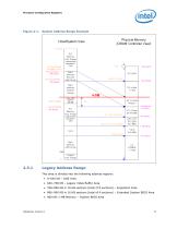
Processor Configuration Registers Figure 2-1. System Address Range Example Host/System View Physical Memory (DRAM Controller View) TOUUD BASE Reclaim Limit - Reclaim BASE TOLUD BASE Legacy Address Range This area is divided into the following address regions: • 640-768 KB - Legacy Video Buffer Area • 768-896 KB in 16 KB sections (total of 8 sections) - Expansion Area • 896-960 KB in 16 KB sections (total of 4 sections) - Extended System BIOS Area • 960 KB-1 MB Memory - System BIOS Area
カタログの17ページ目を開く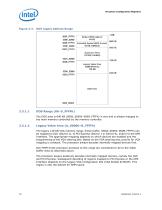
Processor Configuration Registers Figure 2-2. DOS Legacy Address Range OOOF FFFFh System BIOS (Upper) OOOE FFFFh Extended System BIOS (Lower) Expansion Area Legacy Video Area The DOS area is 640 KB (0000_0000h-0009_FFFFh) in size and is always mapped to the main memory controlled by the memory controller. 2.3.1.2 Legacy Video Area (A_OOOOh-B_FFFFh) The legacy 128 KB VGA memory range, frame buffer, (000A_0000h-000B_FFFFh) can be mapped to IGD (Device 2), to PCI Express (Device 1 or Device 6), and/or to the DMI Interface. The appropriate mapping depends on which devices are enabled and the...
カタログの18ページ目を開く
Processor Configuration Registers Compatible SMRAM Address Range (A_0000h–B_FFFFh) When compatible SMM space is enabled, SMM-mode processor accesses to this range route to physical system DRAM at 000A_0000h–000B_FFFFh. PCI Express and DMI originated cycles to enable SMM space are not allowed and are considered to be to the Video Buffer Area, if IGD is not enabled as the VGA device. DMI initiated writes cycles are attempted as peer writes cycles to a VGA enabled PCIe port. Monochrome Adapter (MDA) Range (B_0000h–B_7FFFh) Legacy support requires the ability to have a second graphics...
カタログの19ページ目を開くIntel/インテルのすべてのカタログと技術パンフレット
-
 10th Gen Intel® Core
7 ページ
-
 10th Gen
8 ページ
-
 nuc-celeron
4 ページ
-
 Intel® Ethernet Controller XL710
1726 ページ
-
 Intel® X99 Chipset
4 ページ
-
 S2600GZ and S2600GL
245 ページ
-
 i7-lga2011
314 ページ
-
 c600-series
936 ページ
-
 b75-express
4 ページ
-
 desktop-board
4 ページ
-
 /3rd-gen-core
2 ページ


カタログアーカイブ
-
 Intel® 3450 Chipset
2 ページ


