
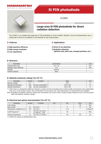
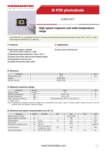
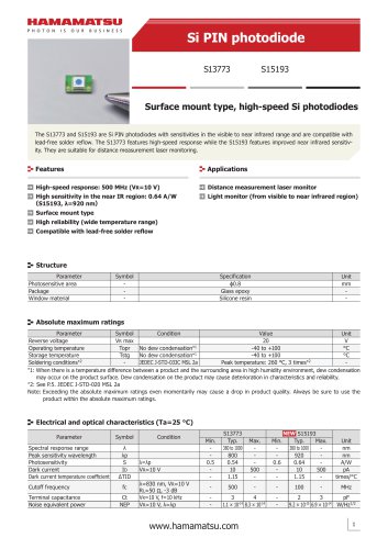
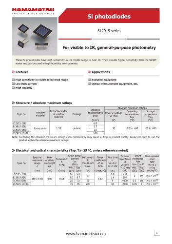
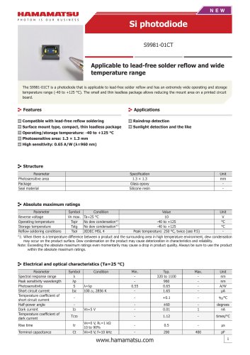
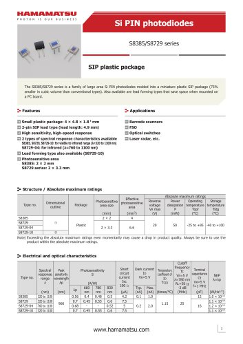
カタログの抜粋

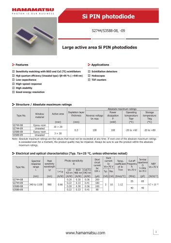
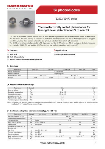
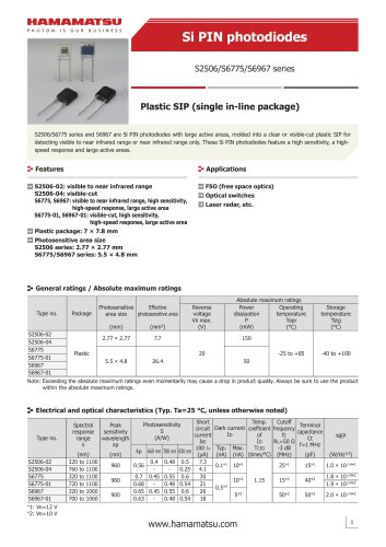
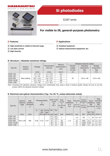
CMOS linear image sensor S14772 High-speed readout (125 klines/s) The S14772 is a CMOS linear image sensor developed for industrial cameras that require high-speed scanning. The columnparallel readout system, which has a readout amplifier and an A/D converter for each pixel, allows high-speed readout. For the A/D converter resolution, either 10-bit (high-speed mode: 125 klines/s max.) or 11-bit (low-speed mode: 62.5 klines/s max.) can be selected. Video signal is output serially in 225 MHz LVDS format. Machine vision Film inspection High-speed readout: 125 klines/s Printed circuit board appearance inspection Simultaneous integration of all pixels Print inspection 3.3 V power supply operation SPI communication function Built-in 10-bit/11-bit A/D converters Structure Parameter Number of pixels Pixel pitch Pixel height Effective photosensitive area length Package Window material*1 Specification 2048 14 14 28.672 Ceramic Borosilicate glass *1: AR coated (1% or less reflectance at 400 to 800 nm) on both sides Absolute maximum ratings (Ta=25 °C) Parameter Symbol Condition Analog terminal Vdd(A) Supply voltage Digital terminal Vdd(D) Counter terminal Vdd(C) Digital input signal terminal voltage*2 Vi Vref_cp1 terminal voltage Vref_cp1 Vref_cp2 terminal voltage Vref_cp2 Operating temperature Topr No dew condensation*3 Storage temperature Tstg No dew condensation*3 *2: CS, SCLK, MOSI, RSTB, MCLK, MST, All-reset, PLL-reset *3: When there is a temperature difference between a product and the surrounding area in high humidity environment, dew condensation may occur on the product surface. Dew condensation on the product may cause deterioration in characteristics and reliability. Note: Exceeding the absolute maximum ratings even momentarily may cause a drop in product quality. Always be sure to use the product within the absolute maximum ratings.
カタログの1ページ目を開く
CMOS linear image sensor Recommended operating conditions (Ta=25 °C) Parameter Analog terminal Digital terminal Supply voltage Counter terminal High level Digital input voltage Low level Symbol Vdd(A) Vdd(D) Vdd(C) Vi(H) Vi(L) Electrical characteristics Digital input signal [Ta=25 °C, Vdd(A)=Vdd(D)=Vdd(C)=3.3 V] Parameter Master clock pulse frequency Master clock pulse duty cycle Master start pulse High-speed mode cycle*4 Low-speed mode Master start pulse High-speed mode High period*4 Low-speed mode Master start pulse High-speed mode Low period*4 Low-speed mode Master clock - Master start...
カタログの2ページ目を開く
CMOS linear image sensor PLL_Reset, All_Reset input timing After 100 μs of turning on the power, set PLL_Reset to low level for at least 5 master clock cycles and then do the same for All_Reset. Rise time of power supply voltage Vdd(A) Vdd(D) Vdd(C) MCLK tCRD Digital output signal [Ta=25 °C, Vdd(A)=Vdd(D)=Vdd(C)=3.3 V, f(MCLK)=37.5 MHz] Parameter Data rate (LVDS) High-speed mode Line rate Low-speed mode Offset LVDS output voltage*7 Differential LVDS rise time*8 LVDS fall time*8 Pclk – OutX[m] delay period Pclk – CTR delay period Rise time Pclk – Sync delay period Fall time High CMOS output...
カタログの3ページ目を開く
CMOS linear image sensor Output timing of Sync signal and video output Pclk Out_X [m] tPDD Sync tPDSR ∙ Each waveform represents the difference between the LVDS positive signal and negative signal. ∙ Out_X[m] is video output. X: A to H (port) m: 0=lower bit, 1=higher bit ∙ Video output should be acquired at the rising timing of Pclk. ∙ Video output starts after the rising of Sync. Sync can be used as reference of data acquisition [refer to Timing chart (P.8)]. ∙ On the rising edge of CTR, the lower bits are output from D0 and the higher bits from D6. CTR can be used as reference of data...
カタログの4ページ目を開く
CMOS linear image sensor Electrical and optical characteristics [Ta=25 °C, Vdd(A)=Vdd(D)=Vdd(C)=3.3 V, f(MCLK)=37.5 MHz, gain: default value, offset: default value, tpi(MST)=8 μs (high-speed mode), 16 μs (low-speed mode)] Common to all modes Parameter Spectral response range Peak sensitivity wavelength Gain=1 Photoresponse nonuniformity*13 Gain=8 Image lag*14 Gain=1 Saturation charge Gain=1 SNR max. Gain=8 *13: The output uniformity when a uniform light with a light exposure that is approximately 50% of saturation output is applied. It is defined as follows for the 2042 pixels excluding the 3...
カタログの5ページ目を開く
CMOS linear image sensor Low-speed mode Parameter Conversion efficiency Saturation output Unit mV DN mV DN mV DN mV DN V/(lx∙s) DN/(lx∙s) V/(lx∙s) DN/(lx∙s) μV/emDN/eμV/emDN/eV DN mV-rms DN-rms mV-rms DN-rms - *15: Measured in the dark state. Difference between the maximum and minimum. *16: Ts=10 ms, voltage difference from the offset output level *17: 2856 K, tungsten lamp *18: Dark state *19: Vsat/Nread Note: DN (digital number): unit of A/D converter output Spectral response (typical example) Spectral transmittance characteristics of window material (Typ. Ta=25 °C)
カタログの6ページ目を開く
CMOS linear image sensor Block diagram The video output signal is divided and output through 8 ports (A through H). Each port outputs 256 pixels of data (pixel numbers output from each port: A=1 to 256, B=257 to 512, ... H=1793 to 2048). Enlarged view of video output (full output mode) Output for each port divides data into LVDS (lower bits and higher bits) pairs. Port A 1 to 256 pixels
カタログの7ページ目を開く
CMOS linear image sensor Timing chart Description of operation The integration time is determined by the low period of the start pulse. MST (1) Integration time Video output (Port A) Integration time Video data Video data Video data Video data Video output (Port B) (1) The start of integration time is determined by the falling edge of the start pulse. (2) The end of integration time is determined by the rising edge of the start pulse. (3) Video data is output after the rising edge of the next start pulse cycle. Video data is output in order from the first pixel. (256 pixels of data are...
カタログの8ページ目を開く
CMOS linear image sensor Example: Port A Full output mode Pclk Sync CTR Out_A[0] 1st pixel 2nd pixel 3rd pixel data data data Invalid data 1/2 output mode Pclk Sync 4 cycles CTR Out_A[0] Invalid data Operation example Example 1 Line rate=125 kline/s, master clock pulse frequency=37.5 MHz, high-speed mode, full output mode, integration time max. MST pulse cycle: 8 μs Integration time: 6.4 μs Sync 6.83 μs Video output ∙ Master start pulse cycle = 300/f(MCLK) = 8 μs (equals the reciprocal of start pulse interval) ∙ Master start pulse’s low period = Master start pulse cycle - Master start...
カタログの9ページ目を開くHAMAMATSUのすべてのカタログと技術パンフレット
-
 PHOTON COUTING HEAD
4 ページ
-
 FLAT PANEL TYPE
4 ページ
-
 SPAD MODULES
5 ページ
-
 LIGHTNINGCURE
29 ページ
-
 Xenon Flash Lamps
19 ページ
-
 ORCA-FUSION C14440-20UP
12 ページ
-
 NanoZommer series
8 ページ
-
 C13410 series
4 ページ
-
 C13410-06A
4 ページ
-
 PMA-12
8 ページ
-
 L12542
4 ページ
-
 FLAT EXCIMER
16 ページ
-
 Optical Gauge series
23 ページ
-
 L15208-01
3 ページ
-
 L15856-01
3 ページ
-
 L14001-01
2 ページ
-
 L11854-336-05
2 ページ
-
 L14351-02
4 ページ
-
 GC-113A
2 ページ
-
 IMAGEMX2 series
8 ページ
-
 ORCA-Fusion BT
9 ページ
-
 DIUTHAME
12 ページ
-
 J12853
2 ページ
-
 J12432-01
2 ページ
-
 J10919 SERIES
2 ページ
-
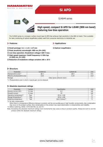 Si APD S14644 series
6 ページ
-
 C15780-401
4 ページ
-
 H15460-40
4 ページ
-
 R14755U-100
2 ページ
-
 Photo IC for rangefinder
14 ページ
-
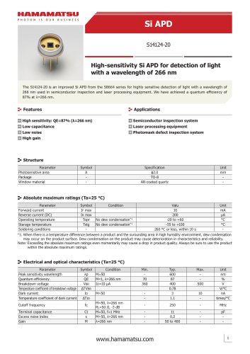 Si APD S14124-20
3 ページ
-
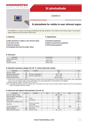
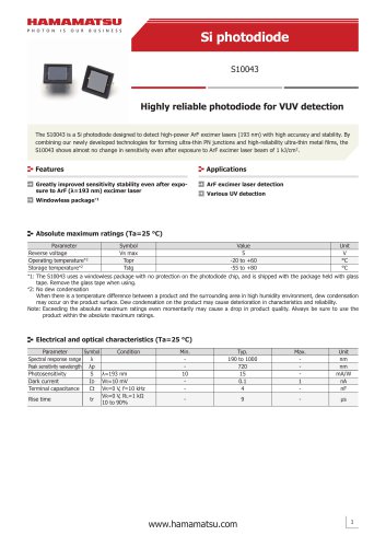 Si photodiode S10043
3 ページ
-
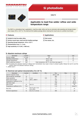 Si photodiode S9674
5 ページ
-
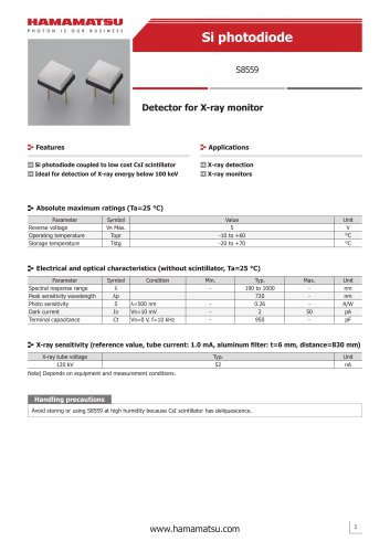 Si photodiode S8559
3 ページ
-
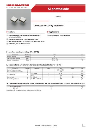 Si photodiode 8193
3 ページ
-
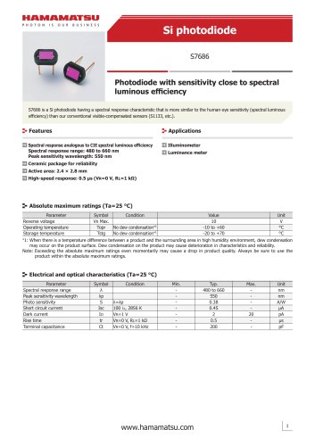 Si photodiode S7686
4 ページ
-
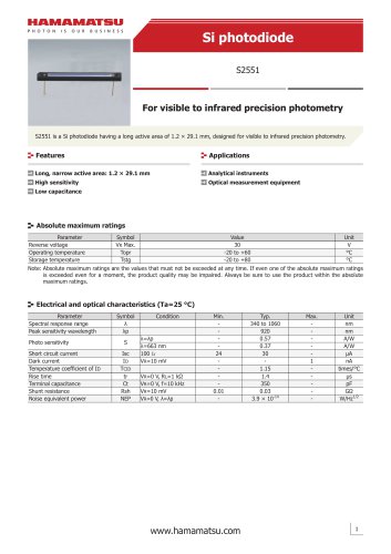 Si photodiode S2551
4 ページ
-
 C13398 series
5 ページ
-
 InGaAs Image sensors
17 ページ
-
 Si APD S14645 series
6 ページ
-
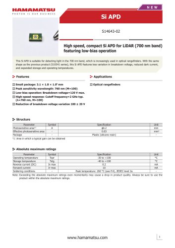 Si APD S14643-02
6 ページ
-
 MEMS mirror S13124-01
10 ページ
-
 LIGHT SOURCES
23 ページ
-
 PHOTOTUBES
8 ページ
-
 FLAME SENSOR UVTRON
4 ページ
-
 PSD
PSD8 ページ
-
 InGaAs Photodiodes
20 ページ
-
 Infrared Detectors
36 ページ
-
 Photo IC
8 ページ
-
 Image Sensors
48 ページ
-
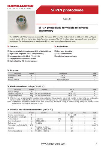
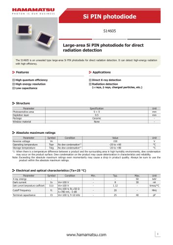
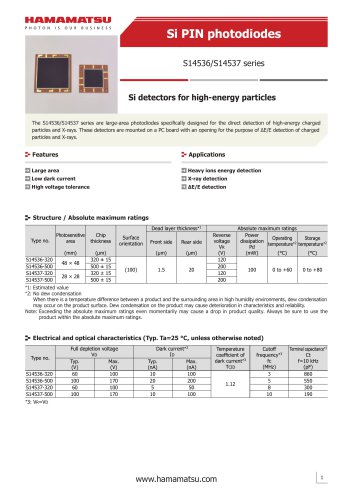
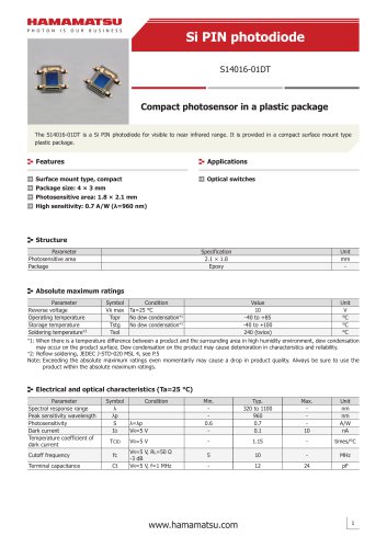
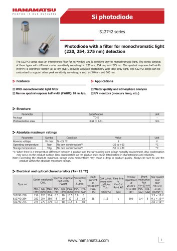
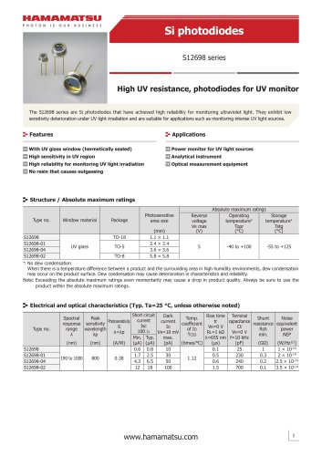
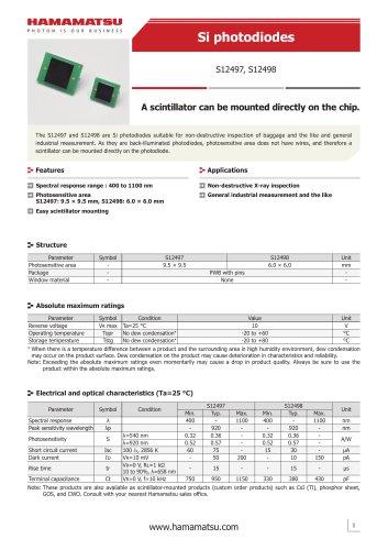
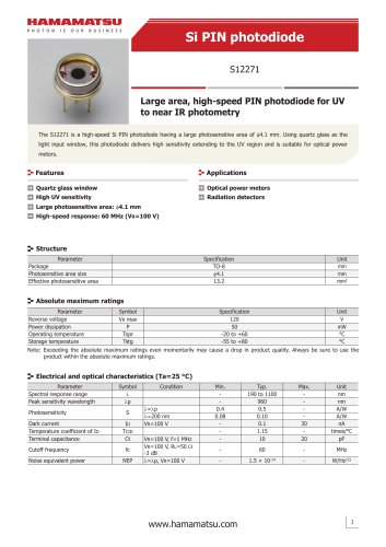
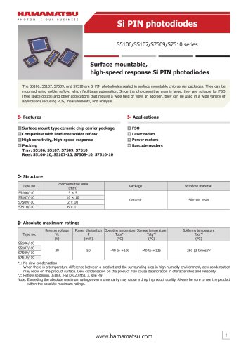
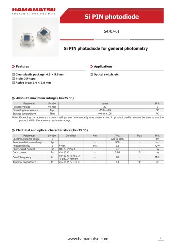
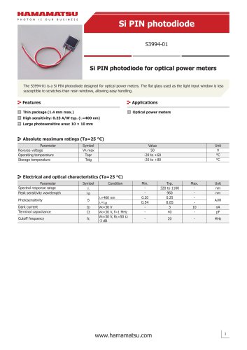
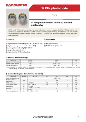
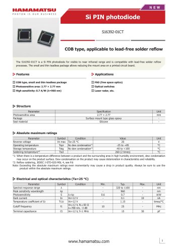
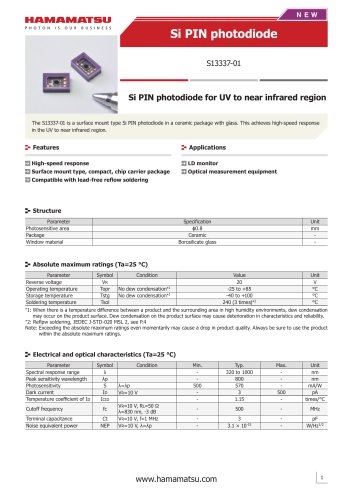
 Si Photodiodes
48 ページ
-
 Si APD
16 ページ
-
 MPPC®, MPPC modules
34 ページ
-
 Photonic Devices
44 ページ
-
 IMAGE INTENSIFIERS
20 ページ
-
 FLOW CELLS
4 ページ
-
 COMPACT HIGH VOLTAGE
2 ページ
-
 SCANBLOCK C10516
4 ページ
-
 UV TRONR DRIVING
2 ページ
-
 High sensitivity
2 ページ
-
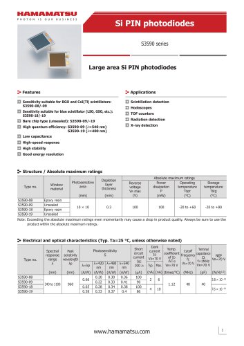
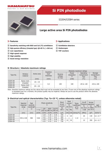
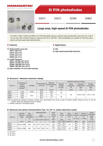
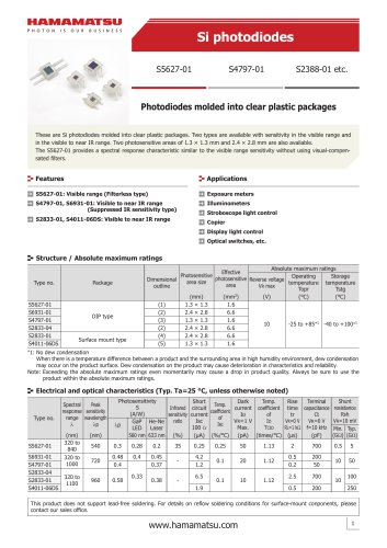
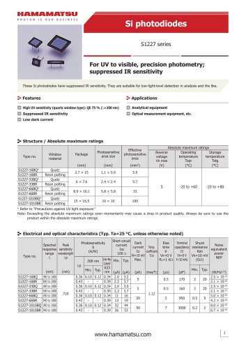
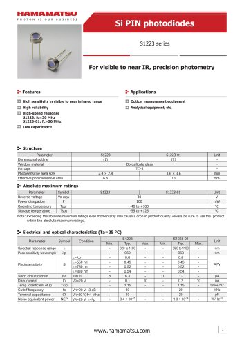
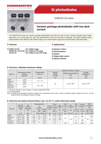
 Si photodiodes
41 ページ


カタログアーカイブ
-
 Opto-semiconductor Catalog
38 ページ


