
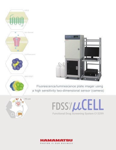
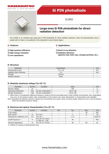
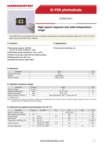
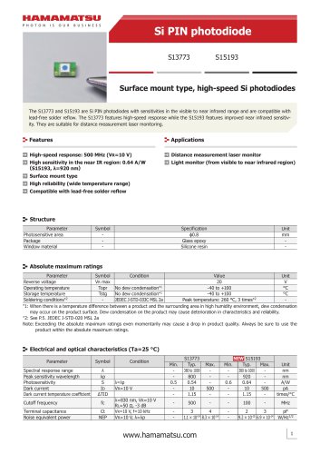
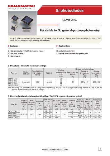
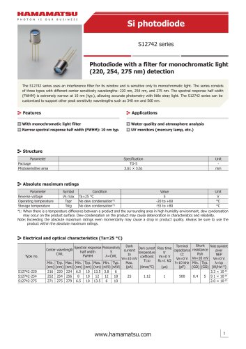
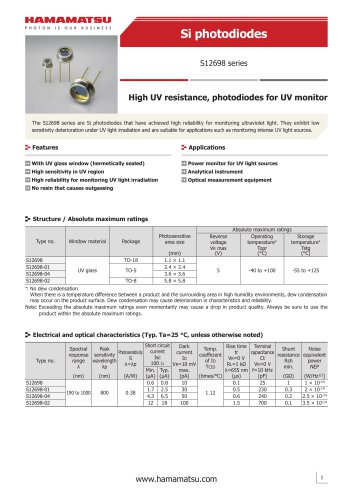
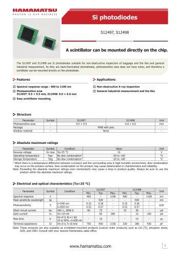
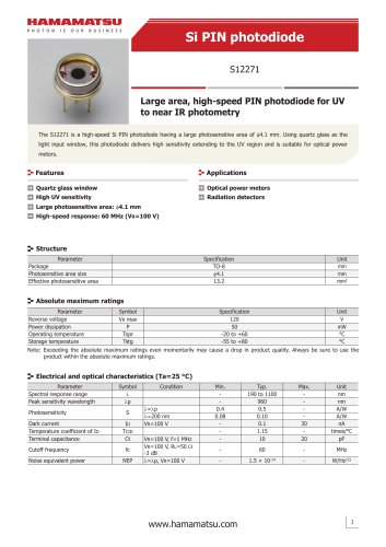
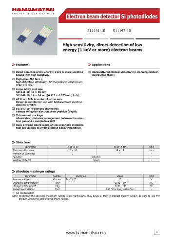
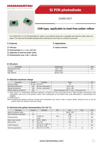
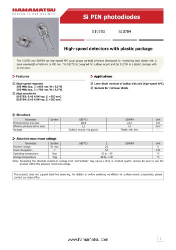
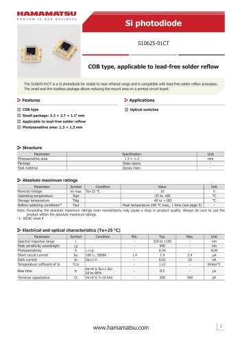
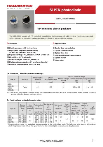
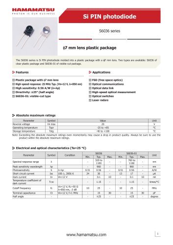
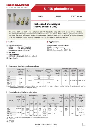
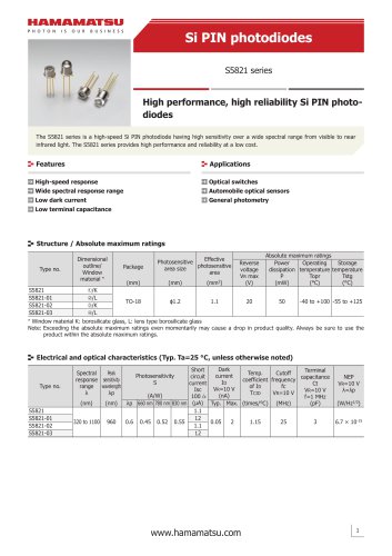
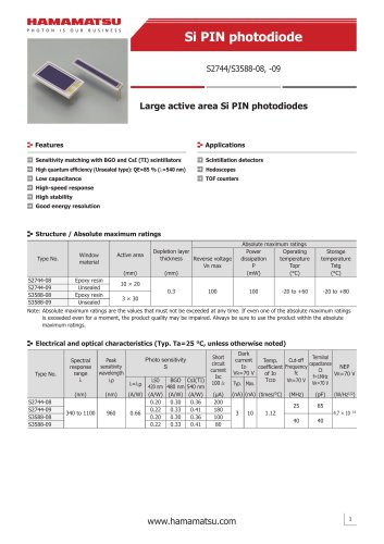
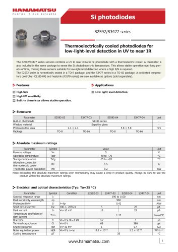
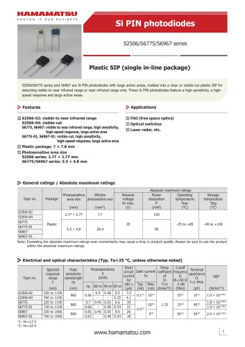
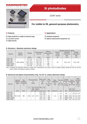
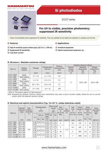
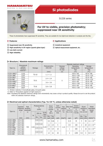
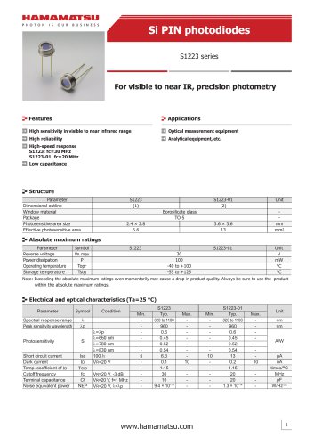
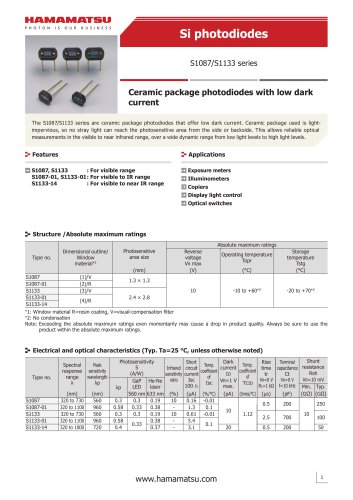
カタログの抜粋

CCD image sensors S11071/S10420-01 series Improved etaloning characteristics, High-speed type and low noise type available The S11071/S10420-01 series are back-thinned CCD image sensors designed for spectrometers. Two types consisting of a high-speed type (S11071 series) and low noise type (S10420-01 series) are available with improved etaloning characteristics. The S11071/S10420-01 series offer nearly flat spectral response characteristics with high quantum efficiency from the UV to near infrared region. Improved etaloning characteristics High sensitivity over a wide spectral range and nearly flat spectral response characteristics High CCD node sensitivity: 8 μV/e- (S11071 series) 6.5 μV/e- (S10420-01 series) High full well capacity and wide dynamic range (with anti-blooming function) Pixel size: 14 × 14 μm Number of effective Image size pixels [mm (H) × mm (V)] 1024 1024 2048 2048 1024 1024 2048 Suitable driver circuit
カタログの1ページ目を開く
Improved etaloning characteristics Etaloning characteristics (typical example) (Ta=25 °C) Etaloning-improved type Relative sensitivity (%) Etaloning is an interference phenomenon that occurs when the light incident on a CCD repeatedly reflects between the front and back surfaces of the CCD while being attenuated, and causes alternately high and low sensitivity. When long-wavelength light enters a back-thinned CCD, etaloning occurs due to the relationship between the silicon substrate thickness and the absorption length. The S11071/S10420-01 series back-thinned CCDs have achieved a significant...
カタログの2ページ目を開く
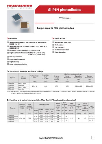
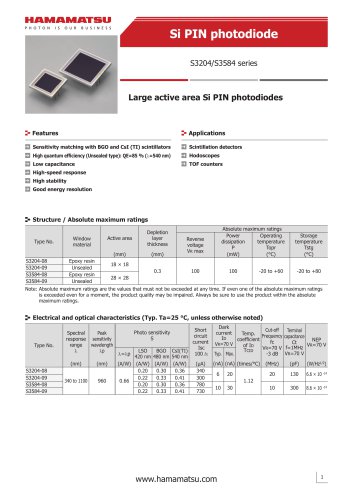
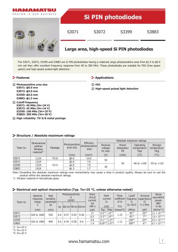
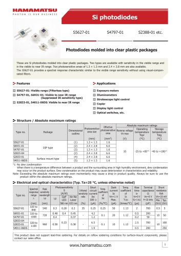
Absolute maximum ratings (Ta=25 °C) Parameter Operating temperature*3 Storage temperature S11071 series Output transistor drain voltage S10420-01 series Reset drain voltage Output amplifier return voltage Overflow drain voltage Vertical input source voltage Horizontal input source voltage Overflow gate voltage Vertical input gate voltage Horizontal input gate voltage Summing gate voltage Output gate voltage Reset gate voltage Transfer gate voltage Vertical shift register clock voltage Horizontal shift register clock voltage Symbol Topr Tstg VRD Vret VOFD VISV VISH VOFG VIG1V, VIG2V VIG1H,...
カタログの3ページ目を開く
Electrical characteristics (Ta=25 °C) Parameter 5 Signal output frequency* -1004(-01) -1006(-01) Vertical shift register capacitance -1104(-01) -1106(-01) Horizontal shift register -1004(-01)/-1006(-01) capacitance -1104(-01)/-1106(-01) Summing gate capacitance Reset gate capacitance -1004(-01)/-1006(-01) Transfer gate capacitance -1104(-01)/-1106(-01) Charge transfer efficiency*6 DC output level*5 Output impedance*5 Power consumption*5 *7 *5: The values depend on the load resistance. (S11071 series: VOD=15 V, RL=2.2 kΩ, S10420-01 series: VOD=24 V, RL=100 kΩ) *6: Charge transfer efficiency per...
カタログの4ページ目を開く
Spectral transmittance characteristic of window material Spectral response (typical example, without window)*13 (Typ. Ta=25 °C) Quantum efficiency (%) *13: Spectral response with quartz glass is decreased according to the spectral transmittance characteristic of window material. Dark current vs. temperature (Typ.) Dark current (e-/pixel/s)
カタログの5ページ目を開く
Device structure (conceptual drawing of top view in dimensional outline) S11071 series Effective pixels Thinning Effective pixels Horizontal shift register 4 blank pixels Horizontal shift register Note: When viewed from the light input side, the horizontal shift register is covered by the thick area of the silicon (insensitive area), but long-wavelength light may pass through the insensitive silicon area. This light may be received by the horizontal shift register. Take measures such as shielding the light. KMPDC0343EC S10420-01 series Effective pixels Thinning Effective pixels Horizontal...
カタログの6ページ目を開く
Timing chart (line binning) Integration time (shutter has to be open) Vertical binning period Readout period (shutter has to be closed) (shutter has to be closed) 3...21 22←16 + 6 (bevel): S11071/S10420-1004, -1104 Tpwv 3...69 70←64 + 6 (bevel): S11071/S10420-1006, -1106 1 2 Tovr P2V, TG Tpwh, Tpws Tovrh 1 Pulse width* Rise and fall times*14 Pulse width*14 Rise and fall times*14 Pulse overlap time Duty ratio*14 Pulse width*14 Rise and fall times*14 Pulse overlap time Duty ratio*14 Pulse width Rise and fall times Overlap time Tpwv Tprv, Tpfv Tpwh Tprh, Tpfh Tovrh Tpws Tprs, Tpfs Tovrh Tpwr...
カタログの7ページ目を開く
Dimensional outline (unit: mm) S11071 series, S10420-1004-01/-1006-01/-1104-01/-1106-01 3.3 ± 0.35 Index mark Photosensitive surface Photosensitive area * Glass thickness (refractive index≈1.5) KMPDA0223EF Photosensitive surface Index mark
カタログの8ページ目を開く
Function Output transistor source Output transistor drain Output gate Summing gate Output amplifier return Reset drain CCD horizontal register clock-4 CCD horizontal register clock-3 CCD horizontal register clock-2 CCD horizontal register clock-1 Test point (horizontal input gate-2) Test point (horizontal input gate-1) Over flow gate Over flow drain Test point (horizontal input source) Test point (vertical input source) Substrate Reset drain Test point (vertical input gate-2) Test point (vertical input gate-1) CCD vertical register clock-2 CCD vertical register clock-1 Transfer gate Reset gate...
カタログの9ページ目を開く
Precautions (electrostatic countermeasures) Electrostatic countermeasures ・ Handle these sensors with bare hands or wearing cotton gloves. In addition, wear anti-static clothing or use a wrist band with an earth ring, in order to prevent electrostatic damage due to electrical charges from friction. ・ Avoid directly placing these sensors on a work-desk or work-bench that may carry an electrostatic charge. ・Provide ground lines or ground connection with the work-floor, work-desk and work-bench to allow static electricity to discharge. ・ Ground the tools used to handle these sensors, such as...
カタログの10ページ目を開く
Information described in this material is current as of December 2019. Product specifications are subject to change without prior notice due to improvements or other reasons. This document has been carefully prepared and the information contained is believed to be accurate. In rare cases, however, there may be inaccuracies such as text errors. Before using these products, always contact us for the delivery specification sheet to check the latest specifications. The product warranty is valid for one year after delivery and is limited to product repair or replacement for defects discovered...
カタログの11ページ目を開くHAMAMATSUのすべてのカタログと技術パンフレット
-
 PHOTON COUTING HEAD
4 ページ
-
 FLAT PANEL TYPE
4 ページ
-
 SPAD MODULES
5 ページ
-
 LIGHTNINGCURE
29 ページ
-
 Xenon Flash Lamps
19 ページ
-
 ORCA-FUSION C14440-20UP
12 ページ
-
 NanoZommer series
8 ページ
-
 C13410 series
4 ページ
-
 C13410-06A
4 ページ
-
 PMA-12
8 ページ
-
 L12542
4 ページ
-
 FLAT EXCIMER
16 ページ
-
 Optical Gauge series
23 ページ
-
 L15208-01
3 ページ
-
 L15856-01
3 ページ
-
 L14001-01
2 ページ
-
 L11854-336-05
2 ページ
-
 L14351-02
4 ページ
-
 GC-113A
2 ページ
-
 IMAGEMX2 series
8 ページ
-
 ORCA-Fusion BT
9 ページ
-
 DIUTHAME
12 ページ
-
 J12853
2 ページ
-
 J12432-01
2 ページ
-
 J10919 SERIES
2 ページ
-
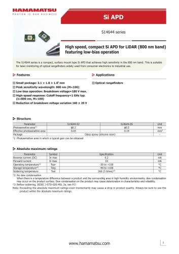 Si APD S14644 series
6 ページ
-
 C15780-401
4 ページ
-
 H15460-40
4 ページ
-
 R14755U-100
2 ページ
-
 Photo IC for rangefinder
14 ページ
-
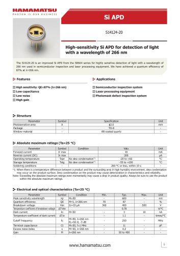 Si APD S14124-20
3 ページ
-
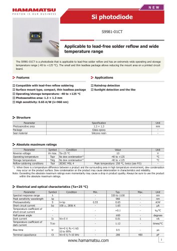
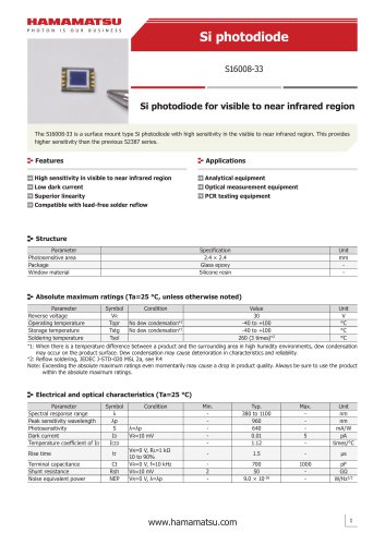
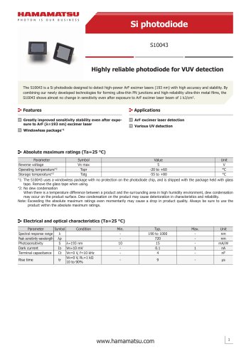 Si photodiode S10043
3 ページ
-
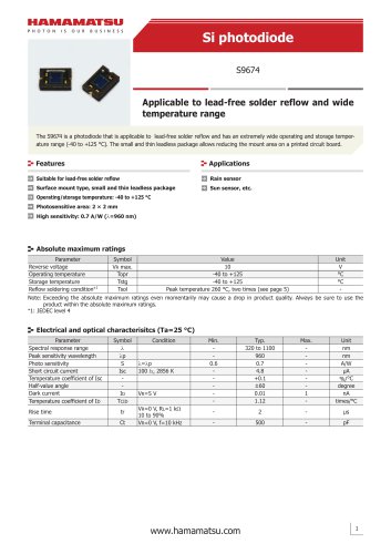 Si photodiode S9674
5 ページ
-
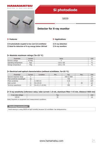 Si photodiode S8559
3 ページ
-
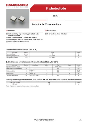 Si photodiode 8193
3 ページ
-
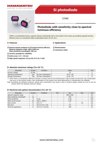 Si photodiode S7686
4 ページ
-
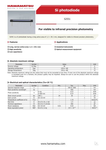 Si photodiode S2551
4 ページ
-
 C13398 series
5 ページ
-
 InGaAs Image sensors
17 ページ
-
 Si APD S14645 series
6 ページ
-
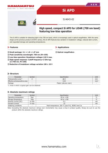 Si APD S14643-02
6 ページ
-
 MEMS mirror S13124-01
10 ページ
-
 LIGHT SOURCES
23 ページ
-
 PHOTOTUBES
8 ページ
-
 FLAME SENSOR UVTRON
4 ページ
-
 PSD
PSD8 ページ
-
 InGaAs Photodiodes
20 ページ
-
 Infrared Detectors
36 ページ
-
 Photo IC
8 ページ
-
 Image Sensors
48 ページ
-
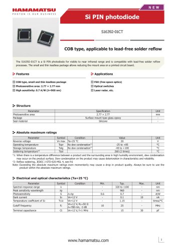
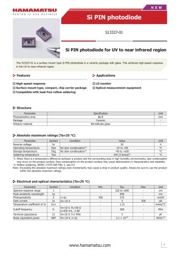
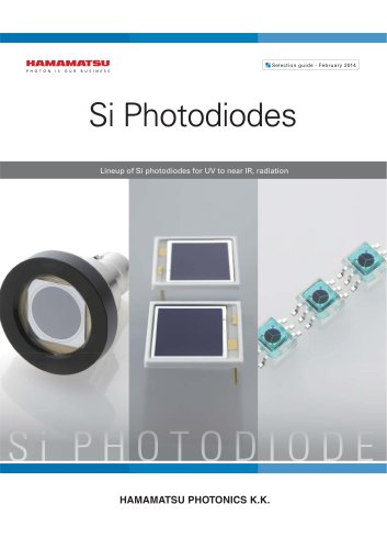 Si Photodiodes
48 ページ
-
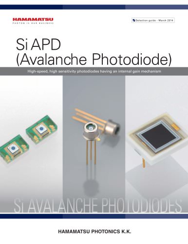 Si APD
16 ページ
-
 MPPC®, MPPC modules
34 ページ
-
 Photonic Devices
44 ページ
-
 IMAGE INTENSIFIERS
20 ページ
-
 FLOW CELLS
4 ページ
-
 COMPACT HIGH VOLTAGE
2 ページ
-
 SCANBLOCK C10516
4 ページ
-
 UV TRONR DRIVING
2 ページ
-
 High sensitivity
2 ページ
-
 Si photodiodes
41 ページ


カタログアーカイブ
-
 Opto-semiconductor Catalog
38 ページ


