
カタログの抜粋
White Paper Thin-Film-Transistor (TFT) LCD Display Control Electronics Design and Operation Revision 1.0 DENSITRON TECHNOLOGIES plc. – PROPRIETARY DATA – ALL RIGHTS RESERVED
カタログの1ページ目を開く
2/17 DENSITRON TECHNOLOGIES plc. – PROPRIETARY DATA – ALL RIGHTS RESERVED
カタログの2ページ目を開く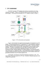
1 TFT OVERVIEW Thin-Film Transistor (TFT) displays are growing in popularity due to their resolution and speed. Today’s LCD televisions and monitors are built using TFT technologies. The structure and operation of a TFT display is shown in Figure 1. Figure 1: TFT LCD structure and operation Figure 1 demonstrates the electrochemical operation characteristics of a TFT display. The drive electronics of a TFT activate the TFT array substrate, resulting in an induced electromagnetic field that affects the liquid crystal. The liquid crystal is twisted in response to the induced E-field, allowing...
カタログの3ページ目を開く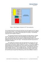
Greyscale Generator Voltage Drive Generator Figure 2: Block Diagram: Elements of TFT drive electronics The Controller logic block controls the instruction and clock signals to the TFT glass’s row and column drivers. The Controller logic block also includes a timing subsection that generates the correct signal cycles to drive the TFT correctly. The Controller logic block will be detailed in Section 2. The Greyscale Generator logic block generates the target reference voltages across a voltage divider circuit to control the brightness and clarity of each color pixel. The Controller logic...
カタログの4ページ目を開く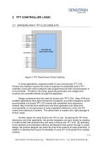
2 TFT CONTROLLER LOGIC 2.1 DRIVERS-ONLY TFT LCD DISPLAYS Figure 3: TFT Row/Column Driver Interface In some applications, engineers prefer to use a drivers-only TFT LCD. Drivers-only interface requires the product engineers to essentially build a TFT controller circuit with control software code programmed into their microprocessor or microcontroller. Therefore, the timing, greyscale generation and voltage drive functions are controlled directly through the application. Design constraints drive the need for drivers-only TFT LCDs. Many PDA and portable applications have tight mechanical...
カタログの5ページ目を開く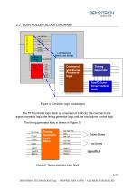
2.2 CONTROLLER BLOCK DIAGRAM Greyscale Generator Voltage Drive Generator Command and Signal Processor logic Timing Generator Row/Column Driver Control block Figure 4: Controller logic subsections The TFT controller logic block is comprised of 3 blocks; the command and signal processor logic, the timing generator logic and the row/column control logic. The timing generator logic is shown in Figure 5. Timing Generator Logic Block Figure 5: Timing generator logic block 6/17 DENSITRON TECHNOLOGIES plc. – PROPRIETARY DATA – ALL RIGHTS RESERVED
カタログの6ページ目を開く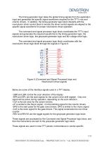
The timing generator logic takes the global timing signals from the application input and generates the specific signal waveforms required for the TFT’s row and column drivers. In addition, the timing generator logic block interacts with the row/column driver control block to ensure the driver control signals are aligned to the specific signal waveforms for proper row/column driver operation. The command and signal processor logic block coordinates the TFT’s input signals and generates the required waveforms to the timing generator logic, the row/column driver logic, the greyscale generator...
カタログの7ページ目を開く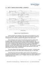
2.3 INPUT TIMING WAVEFORMS - EXAMPLE Figure 6: Input Timing Waveforms These waveforms are examples of the required input waveforms for a TFT with built-in controller. Most TFT displays offer the choice of portrait or landscape mode graphics; the waveforms depend on the graphic mode used as well. Since landscape mode require more horizontal pixels than portrait mode, it requires longer instruction cycle times. Note the differences between the horizontal-portrait (top) and horizontal-landscape (middle) waveforms. Most of the instructions, including the RGB inputs, are the same, except for...
カタログの8ページ目を開く
3 GREYSCALE GENERATOR/PANEL STABILITY 3.1 Greyscale Generator Voltage Drive Generator Figure 7: Greyscale Generator Circuit, with the voltage latch and summing amplifier circuitry inside the column drivers Figure 7a is an example of the greyscale generator circuit. The greyscale generator consists of an op-amp network that generates distinct V0-V4 voltages. These V0-V4 voltages are then paralleled into the summing amplifier circuits (D/A converter circuits) of the column drivers. In general, the voltage relationship is as follows: 9/17 DENSITRON TECHNOLOGIES plc. – PROPRIETARY DATA – ALL...
カタログの9ページ目を開く
V0 < V1 < V2 < V3 < V4 Each D/A converter circuit has a data latch that releases V0-V4 to the summing amplifier according to the instructions from the Controller logic block. The output of the D/A converter circuit sets the voltage applied to a specific cell to control the ‘brightness’ level of the individual pixel. Note that the levels of brightness and color available are dependent on the complexity of the column drivers. Although a TFT LCD panel’s input waveforms may indicate a digital device, the glass panel is not. The liquid crystal lattice reacts to AC voltage waveforms; therefore,...
カタログの10ページ目を開く
PANEL STABILITY (REV and VCOM) In Figure 7b, REV and VCOM can be seen to influence the Gamma Curve. However, REV and VCOM play another, more critical, role in a TFT panel operation – to ensure the TFT panel maintain net zero DC voltage throughout its operation. Please note REV is used to generate VCOM. Figure 8 shows the top-level REV/VCOM block diagrams and the circuitry in a TFT panel. Controller Block Controller Block Controller Block Figure 8: REV and the corresponding generated VCOM signal Figure 8a shows the high-level block diagram of the role of REV and VCOM signals. The DC offset...
カタログの11ページ目を開く
Figure 9: VCOM circuit: DC offset, VCOM adjustment, and VEE modulation Figure 9 shows a typical VCOM circuit. VCOM needs to be adjusted to match the capacitance and performance specifications of the TFT panel to maximize contrast and minimize flickering. Therefore, the VCOM circuit is tweaked during panel production to ensure consistent performance. Note that in Figure 9’s example, the circuit is constructed to output a typical +1.1V DC Offset. In reality, panels sometimes require a net DC offset to achieve optimum performance due to impurities and other production issues. In addition, VCOM...
カタログの12ページ目を開くDensitron Technologiesのすべてのカタログと技術パンフレット
-
 DensiTouchTM
16 ページ


カタログアーカイブ
-
 New 1.69" OLED
1 ページ
-
 Touch Screens
1 ページ
-
 New 0.96" OLED
1 ページ
-
 New 7" TFT
1 ページ
-
 Corporate Statement
2 ページ
-
 Composite Video
1 ページ
-
 Monographic Displays
2 ページ
-
 EL Displays
1 ページ
-
 CSTN
CSTN4 ページ
-
 TFT Displays
4 ページ
-
 OLED Displays
2 ページ
-
 Evaluation Kits
2 ページ
-
 Open Frame Monitors
2 ページ
-
 OLED
OLED2 ページ

