
カタログの抜粋
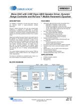
WM9081 Mono DAC with 2.6W Class AB/D Speaker Driver, Dynamic Range Controller and ReTune™ Mobile Parametric Equalizer DESCRIPTION The WM9081 is designed to provide high power output at low distortion levels in space-constrained portable applications. ReTuneTM Mobile Parametric EQ with fully programmable coefficients is integrated for optimization of speaker characteristics. Programmable dynamic range control is also available for maximizing loudness, protecting speakers from clipping and preventing premature shutdown due to battery droop. Digital input enables the power drivers to be located close to the speakers in multi-channel systems without the need for troublesome long analogue connections. Location of the power drivers close to the speakers also removes the need for bulky and expensive class D filters and reduces PCB track lengths, minimising emissions. The digital input can also help to minimise crosstalk to the speaker output signal from high gain microphone inputs, enhancing stability and reducing the risk of ‘howling’ during speakerphone operation. Four control interface addresses and four-channel TDM are supported to allow multiple devices to be configured and driven independently. The device is controlled via a standard 2-wire, 3-wire, or 4wire control interface or by hardware control pins. High-power, high performance DAC and speaker driver 92dB SNR (‘A-weighted’) in Class D mode 97dB SNR (‘A-weighted’) in Class AB mode <0.05% THD+N @0.5W continuous into 4Ω (Class D) <0.10% THD+N @2W continuous into 4Ω (Class D) 2.6W maximum peak power ReTuneTM Mobile Parametric Equalizer Fully programmable filter coefficients Programmable dynamic range controller Boosts small signals to maximise loudness Protects against battery droop and clipping Speaker common mode boost Maximises power for a given SPKVDD/AVDD ratio Low power FLL Provides all necessary internal clocks 32kHz to 27MHz input frequency All common sample rates from 8kHz to 96kHz supported Standard 2-wire, 3-wire, 4-wire and hardware control modes Data formats: LJ, RJ, I2S, DSP, all with TDM support Thermal shutdown interrupt 4x4 COL package (0.45mm lead pitch) Operating temperature range: -40°C to 85°C Portable navigation systems Mobile phones Flat panel TVs BLOCK DIAGRAM DBVDD SPKVDD SPKGND +6dB to -57dB, 1dB steps IN2 ___ CS/ADDR1/4FS SCLK SDIN/ENA SDOUT/ADDR0 SCIM/CHANNEL SWMODE ___ IRQ DIGITAL FILTERS VOLUME CONTROL CONTROL INTERFACE SPKOUTP SPKOUTN PARAMETRIC EQ DYNAMIC RANGE CONTROLLER DACDAT BCLK LRCLK DIGITAL AUDIO INTERFACE CLOCK CONTROL Voltage Reference
カタログの1ページ目を開く
LRCLK DACDAT DCVDD DBVDD DGND SWMODE SCIM/CHANNEL ORDERING INFORMATION Note: Reel quantity = 3500
カタログの3ページ目を開く
WM9081 ABSOLUTE MAXIMUM RATINGS Absolute Maximum Ratings are stress ratings only. Permanent damage to the device may be caused by continuously operating at or beyond these limits. Device functional operating limits and guaranteed performance specifications are given under Electrical Characteristics at the test conditions specified. ESD Sensitive Device. This device is manufactured on a CMOS process. It is therefore generically susceptible to damage from excessive static voltages. Proper ESD precautions must be taken during handling and storage of this device. Cirrus Logic tests its package...
カタログの5ページ目を開く
WM9081 ELECTRICAL CHARACTERISTICS COMMON TEST CONDITIONS Unless otherwise stated, the following test conditions apply throughout the following sections: • DCVDD = DBVDD = 1.8V, AVDD = 3.3V, SPKVDD = 5.0V • PGA gain = 0dB • ACGAIN=DCGAIN=1.52 • Audio signal: 1kHz sine wave, sampled at 48kHz with 24-bit data resolution, I2S mode • Ambient temperature: TA = +25°C • VMID_SEL[1:0] = 01 (2x40kO) Additional, specific test conditions are given within the relevant sections below. 1. Signal-to-Noise Ratio (dB) - SNR is a measure of the difference in level between the maximum theoretical full scale...
カタログの6ページ目を開く
ANALOGUE REFERENCE LEVELS
カタログの8ページ目を開く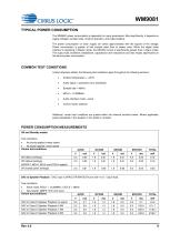
WM9081 TYPICAL POWER CONSUMPTION The WM9081 power consumption is dependent on many parameters. Most significantly, it depends on supply voltages, sample rates, mode of operation, and output loading. The power consumption on each supply rail varies approximately with the square of the voltage. Power consumption is greater at fast sample rates than at slower ones. When the digital audio interface is operating in Master mode, the DBVDD current is significantly greater than in Slave mode. The output load conditions (impedance, capacitance and inductance) can also impact significantly on the...
カタログの9ページ目を開く
CIRRUS LOGIC WM9081 DAC to Lineout Playback - DAC input to LINEOUT pin with 10kO load. Test conditions: • Slave mode, MCLK = 12.288MHz, LRCLK = 48kHz • Input signal: 0dBFS 1kHz sine wave
カタログの10ページ目を開く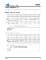
SPEAKER CLASS D INTO 4Q + 10^H Sweep Trace Color Line Style Thick Data Axis Comment Anlr.TTHD+N Ratio Left Anlr.TTHD+N Ratio Left Anlr.TTHD+N Ratio Left Anlr.TTHD+N Ratio Left SPKVDD = 5.0V, AVDD = 3.3V, DCGAIN = ACGAIN = 3.6dB SPKVDD = 4.2V, AVDD = 3.3V, DCGAIN = ACGAIN = 2.1dB SPKVDD = 3.7V, AVDD = 3.0V, DCGAIN = ACGAIN = 2.1dB SPKVDD = 3.3V, AVDD = 3.3V, DCGAIN = ACGAIN = 0dB Device: WM9081 MMC=WPF Input Signal: 1KHz; 0dBFS; 24-bit; 256fs (fs=48kHz) Output Path: SPK Class D Supplies: DBVDD=DCVDD=3.3V BW Filter: 22Hz to 20kHz AES17 Additional Filtering: none Load = 4R1 +...
カタログの11ページ目を開く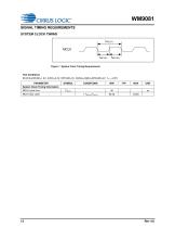
WM9081 SIGNAL TIMING REQUIREMENTS SYSTEM CLOCK TIMING tMCLKY MCLK tMCLKL Figure 1 System Clock Timing Requirements Test Conditions DCVDD=DBVDD=1.8V, AVDD=3.3V, SPKVDD=5V, DGND=AGND=SPKGND=0V, TA = +25oC PARAMETER System Clock Timing Information MCLK cycle time MCLK duty cycle
カタログの12ページ目を開く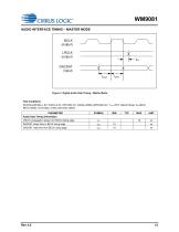
WM9081 AUDIO INTERFACE TIMING - MASTER MODE BCLK (output) LRCLK (output) DACDAT (input) Figure 2 Digital Audio Data Timing - Master Mode Test Conditions DCVDD=DBVDD=1.8V, AVDD=3.3V, SPKVDD=5V, DGND=AGND=SPKGND=0V, TA=+25oC, Master Mode, fs=48kHz, MCLK=256fs, 24-bit data, unless otherwise stated.
カタログの13ページ目を開く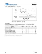
WM9081 AUDIO INTERFACE TIMING - SLAVE MODE BCLK (input) LRCLK (input) DACDAT (input) Figure 3 Digital Audio Data Timing - Slave Mode Test Conditions DCVDD=DBVDD=1.8V, AVDD=3.3V, SPKVDD=5V, DGND=AGND=SPKGND=0V, TA=+25oC, Slave Mode, fs=48kHz, MCLK=256fs, 24-bit data, unless otherwise stated. Note: BCLK period should always be greater than or equal to MCLK period.
カタログの14ページ目を開くCirrus Logicのすべてのカタログと技術パンフレット
-
 CS5343/44
21 ページ
-
 WM0011
233 ページ
-
 CS4970x4
31 ページ
-
 CS4953xx
37 ページ
-
 CS42L51
84 ページ
-
 CS42L42
184 ページ
-
 CS43198
137 ページ
-
 CS43131
156 ページ
-
 CS43130
137 ページ
-
 CS5351
23 ページ
-
 CS5346
38 ページ
-
 CS5341/42
21 ページ
-
 CS35L32
51 ページ
-
 CS35L00/01/03
34 ページ


カタログアーカイブ
-
 CS48DV2/6
2 ページ


