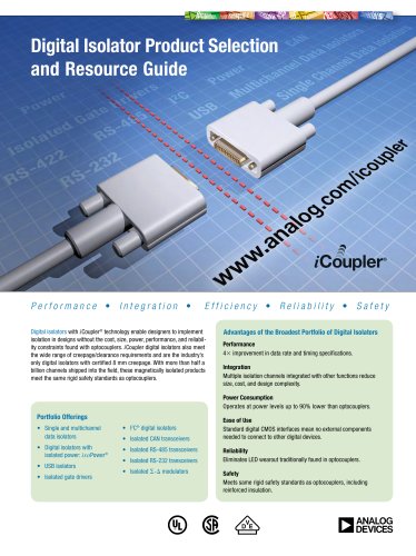
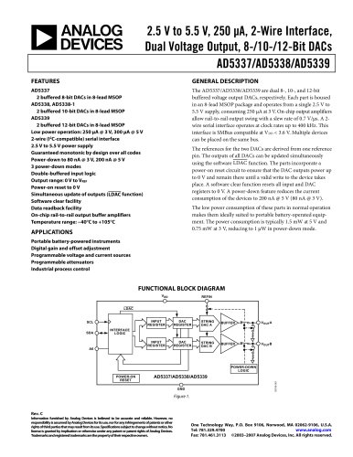
カタログの抜粋
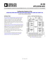
AN-698 APPLICATION NOTE One Technology Way • P.O. Box 9106 • Norwood, MA 02062-9106, U.S.A. • Tel: 781.329.4700 • Fax: 781.461.3113 • www.analog.com Configuration Registers of the ADM1062/ADM1063/ADM1064/ADM1065/ADM1066/ ADM1067/ADM1166 by Peter Canty and Michael Bradley This application note briefly outlines the functions of the devices and provides details of the registers required to set up device configuration. CLOSED LOOP MARGINING SYSTEM VX1 CONFIGURABLE OUTPUT DRIVERS DUAL FUNCTION INPUTS CONFIGURABLE OUTPUT DRIVERS PROGRAMMABLE RESET GENERATORS (LV-CAPABLE OF DRIVING LOGIC SIGNALS) Figure 1. ADM1066 Functional Block Diagram SEQUENCING ENGINE PDO3 (HV-CAPABLE OF DRIVING GATE OF N-CHANNEL FET) (LOGIC INPUTS OR SFDs) For more information on the features and functions of the ADM1062/ADM1063/ADM1064/ADM1065/ADM1066/ ADM1067/ADM1166, see the relevant data sheets. All features of the ADM1062/ADM1063/ADM1064/ADM1065/ ADM1066/ADM1067/ADM1166 are programmable through an SMBus interface. The devices also contain nonvolatile memory (EEPROM) so that the configuration of these features can be stored on-chip and downloaded on each power-up. SMBus INTERFACE The ADM1062/ADM1063/ADM1064/ADM1065/ADM1066/ ADM1067/ADM1166 family of fully programmable supply sequencers and supervisors can be used as complete supply management solutions in systems using multiple voltage supplies. Such applications include line cards in telecommunications infrastructure equipment (central office, base stations) and blade cards in servers. REFIN REFOUT REFGND SDA SCL A1 A0
カタログの1ページ目を開く
Application Note
カタログの2ページ目を開く
Application Note UPDATING MEMORY, ENABLING BLOCK ERASE, AND DOWNLOADING EEPROM The register/bit map detail in Figure 2 shows the configuration required to This application note contains all of the register information required to configure the many features of the ADM1062/ ADM1063/ADM1064/ADM1065/ADM1066/ADM1067/ ADM1166. The devices contain both volatile and nonvolatile memory, which must be set up correctly if any alterations to the configuration are to be updated properly in the device. The volatile memory of the devices is constructed with double buffered latches. For information on...
カタログの3ページ目を開く
Application Note INPUTS The ADM1062/ADM1063/ADM1064/ADM1065/ADM1066/ ADM1067/ADM1166 devices have 10 inputs. Five of these are dedicated supply fault detectors, highly programmable reset generators whose inputs can detect overvoltage, undervoltage, or out-of-window faults. With these five inputs, voltages from 0.573 V to 14.4 V can be supervised. The undervoltage and overvoltage thresholds can all be programmed to an 8-bit resolution. The comparators used to detect faults on the inputs have digitally programmable hysteresis to provide immunity to supply bounce. Each of these inputs also has...
カタログの4ページ目を開く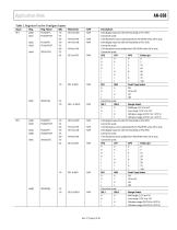
Application Note Table 2. Registers Used to Configure Inputs Input VP1 Description 8-bit digital value for the OV threshold on PS1 SFD. Cannot be used. 5-bit hysteresis to be subtracted from PS1OVTH when OV is true. 8-bit digital value for the UV threshold on PS1 SFD. Cannot be used. 5-bit hysteresis to be added from PS1UVTH when UV is true. Cannot be used. GF2 GF1 GF0 Delay (µs) 0 0 0 0 0 0 1 5 0 1 0 10 0 1 1 20 1 0 0 30 1 0 1 50 1 1 0 75 1 1 1 100 RS1 RS0 Fault Type Select 0 0 OV 0 1 UV or OV 1 0 UV 1 1 Off Cannot be used. SEL1 SEL0 Range Select 0 0 Midrange (2.5 V to 6 V) 0 1 Low range...
カタログの5ページ目を開く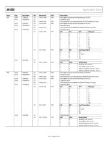
Description 8-bit digital value for the OV threshold on PS3 SFD. Cannot be used. 5-bit hysteresis to be subtracted from PS3OVTH when OV is true. 8-bit digital value for the UV threshold on PS3 SFD. Cannot be used. 5-bit hysteresis to be added from PS3UVTH when UV is true. Cannot be used. GF2 GF1 GF0 Delay (μs) 0 0 0 0 0 0 1 5 0 1 0 10 0 1 1 20 1 0 0 30 1 0 1 50 1 1 0 75 1 1 1 100 RS1 RS0 Fault Type Select 0 0 OV 0 1 UV or OV 1 0 UV 1 1 Off Cannot be used. SEL1 SEL0 Range Select 0 0 Midrange (2.5 V to 6 V) 0 1 Low range (1.25 V to 3 V) 1 0 Ultralow range (0.573 V to 1.375 V) 1 1 Ultralow...
カタログの6ページ目を開く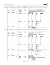
Application Note Input VH Reg. Name PSVHOVTH PSVHOVHYST INVIN INTYP Description 8-bit digital value for the OV threshold on PSVH SFD. Cannot be used. 5-bit hysteresis to be subtracted from PSVHOVTH when OV is true. 8-bit digital value for the UV threshold on PSVH SFD. 5-bit hysteresis to be added from PSVHUVTH when UV is true. Cannot be used. GF2 GF1 GF0 Delay (μs) 0 0 0 0 0 0 1 5 0 1 0 10 0 1 1 20 1 0 0 30 1 0 1 50 1 1 0 75 1 1 1 100 RS1 RS0 Fault Type Select 0 0 OV 0 1 UV or OV 1 0 UV 1 1 Off Cannot be used. SEL0 Range Select 0 Low range (2.5 V to 6.0 V) 1 High range (6.0 V to 14.4 V)...
カタログの7ページ目を開く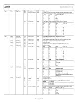
Application Note Reg. Name INVIN INTYP Description Length of pulse output once an edge has been detected on input. PULS1 PULS0 Pulse Length (μs) 0 0 10 0 1 100 1 0 1000 1 1 10,000 Glitch filter. Length of time for which a pulse is ignored. GF2 GF1 GF0 Delay (μs) 0 0 0 0 0 0 1 5 0 1 0 10 0 1 1 20 1 0 0 30 1 0 1 50 1 1 0 75 1 1 1 100 8-bit digital value for the OV threshold on X2 SFD. Cannot be used. 5-bit hysteresis to be subtracted from X2OVTH when OV is true. 8-bit digital value for the UV threshold on X2 SFD. Cannot be used. 5-bit hysteresis to be added from X2UVTH when UV is true. Cannot...
カタログの8ページ目を開く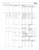
Application Note INVIN INTYP
カタログの9ページ目を開く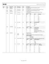
INVIN INTYP Description 8-bit digital value for the OV threshold on X4 SFD. Cannot be used. 5-bit hysteresis to be subtracted from X4OVTH when OV is true. 8-bit digital value for the UV threshold on X4 SFD. Cannot be used. 5-bit hysteresis to be added from X4UVTH when UV is true. Cannot be used. GF2 GF1 GF0 Delay (μs) 0 0 0 0 0 0 1 5 0 1 0 10 0 1 1 20 1 0 0 30 1 0 1 50 1 1 0 75 1 1 1 100 RS1 RS0 Fault Type Select 0 0 OV 0 1 UV or OV 1 0 UV 1 1 Off Cannot be used. SEL1 SEL0 Function Select 0 0 SFD (fault) only 0 1 GPI (fault) only 1 0 GPI (fault) + SFD (warning) No function (input can still...
カタログの10ページ目を開く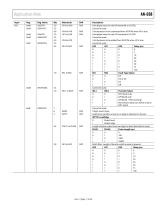
Application Note Input VX5 INVIN INTYP Description 8-bit digital value for the OV threshold on X5 SFD. Cannot be used. 5-bit hysteresis to be subtracted from X5OVTH when OV is true. 8-bit digital value for the UV threshold on X5 SFD. Cannot be used. 5-bit hysteresis to be added from X5UVTH when UV is true. Cannot be used. GF2 GF1 GF0 Delay (μs) 0 0 0 0 0 0 1 5 0 1 0 10 0 1 1 20 1 0 0 30 1 0 1 50 1 1 0 75 1 1 1 100 RS1 RS0 Fault Type Select 0 0 OV 0 1 UV or OV 1 0 UV 1 1 Off Cannot be used. SEL1 SEL0 Function Select 0 0 SFD (fault) only 0 1 GPI (fault) only 1 0 GPI (fault) + SFD (warning) No...
カタログの11ページ目を開くAnalog Devices/アナログ・デバイセズのすべてのカタログと技術パンフレット
-
 HMC722LP3E
8 ページ
-
 HMC853 Data Sheet
10 ページ
-
 AN-1084
8 ページ
-
 AN-1091
2 ページ
-
 AN_737
8 ページ
-
 AN-0982
4 ページ
-
 ADF7024
24 ページ
-
 AD9915
48 ページ
-
 AD9914
48 ページ
-
 ADRF6612
59 ページ
-
 ADRF6820
48 ページ
-
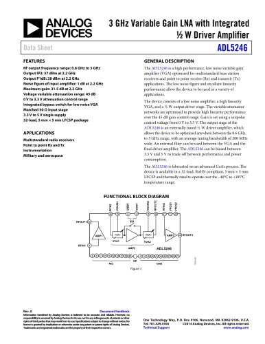
 ADL5246
32 ページ
-
 ADA4961
22 ページ
-
 AN-1141
8 ページ
-
 Temperature Sensors
2 ページ
-
 Reference Circuits
8 ページ
-
 Precision ADCs
16 ページ