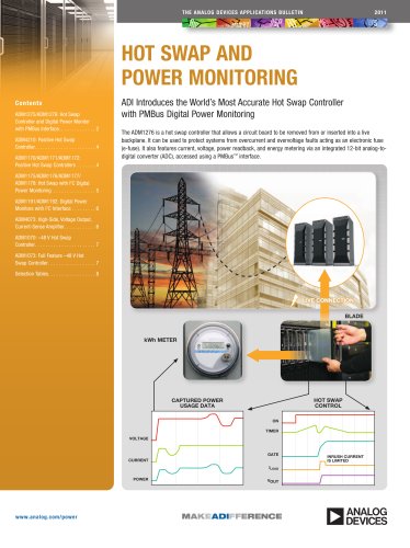
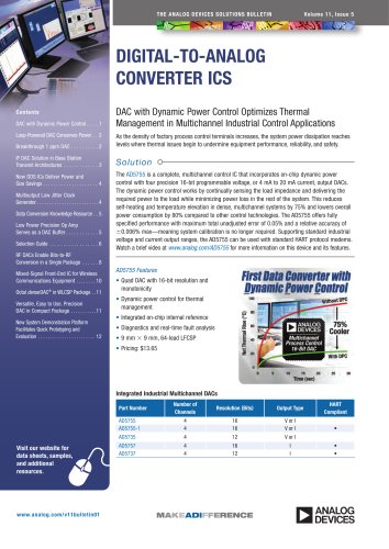
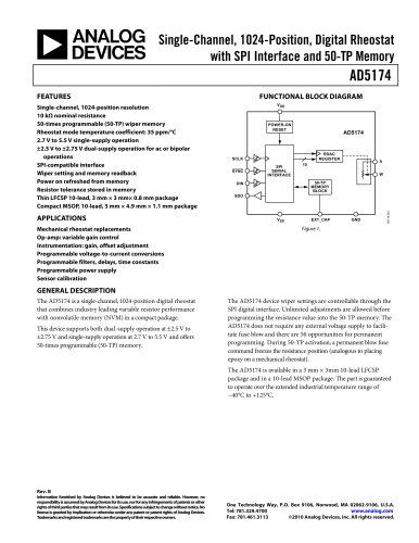
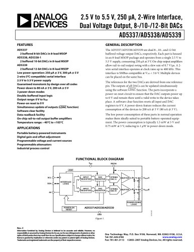
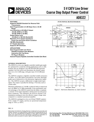
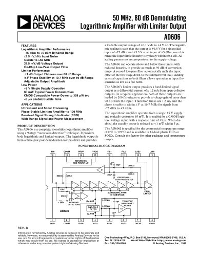
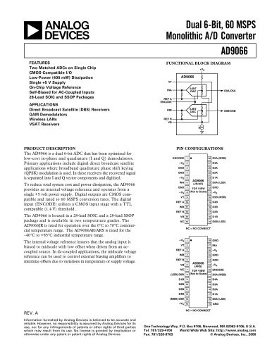
カタログの抜粋

Wideband Quadrature Modulator with Integrated Fractional-N PLL and VCOs ADRF6720 Data Sheet FEATURES GENERAL DESCRIPTION I/Q modulator with integrated fractional-N PLL RF output frequency range: 700 MHz to 3000 MHz Internal LO frequency range: 356.25 MHz to 2855 MHz Output P1dB: 12.2 dBm at 2140 MHz Output IP3: 32.6 dBm at 2140 MHz Carrier feedthrough: −40.3 dBm at 2140 MHz Sideband suppression: −37.6 dBc at 2140 MHz Noise floor: −157.9 dBm/Hz at 2140 MHz Baseband 1 dB modulation bandwidth: >1000 MHz Baseband input bias level: 0.5 V Power supply: 3.3 V/425 mA Integrated RF tunable balun allowing single-ended RF output Multicore integrated VCOs HD3/IP3 optimization Sideband suppression and carrier feedthrough optimization High-side/low-side LO injection Programmable via 3-wire serial port interface (SPI) 40-lead 6 mm × 6 mm LFCSP The ADRF6720 is a wideband quadrature modulator with an integrated synthesizer ideally suited for 3G and 4G communication systems. The ADRF6720 consists of a high linearity broadband modulator, an integrated fractional-N phase-locked loop (PLL), and four low phase noise multicore voltage controlled oscillators (VCOs). The ADRF6720 local oscillator (LO) signal can be generated internally via the on-chip integer-N and fractional-N synthesizers, or externally via a high frequency, low phase noise LO signal. The internal integrated synthesizer enables LO coverage from 356.25 MHz to 2855 MHz using the multicore VCOs. In the case of internal LO generation or external LO input, quadrature signals are generated with a divide-by-2 phase splitter. When the ADRF6720 is operated with an external 1 × LO input, a polyphase filter generates the quadrature inputs to the mixer. The ADRF6720 offers digital programmability for carrier feedthrough optimization, sideband suppression, HD3/IP3 optimization, and high-side or low-side LO injection. APPLICATIONS 2G/3G/4G/LTE broadband communication systems Microwave point-to-point radios Satellite modems Military/aerospace Instrumentation The ADRF6720 is fabricated using an advanced silicongermanium BiCMOS process. It is available in a 40-lead, RoHS-compliant, 6 mm × 6 mm LFCSP package with an exposed pad. Performance is specified over the −40°C to +85°C temperature range. FUNCTIONAL BLOCK DIAGRAM VPOSx 40 LOOUT+ LOOUT– PHASE CORRECTION PHASE CORRECTION SERIAL PORT INTERFACE 31 Document Feedback Information furnished by Analog Devices is believed to be accurate and reliable. However, no responsibility is assumed by Analog Devices for its use, nor for any infringements of patents or other rights of third parties that may result from its use. Specifications subject to change without notice. No license is granted by implication or otherwise under any patent or patent rights of Analog Devices. Trademarks and registered trademarks are the property of their respective owners. One Technology Way, P.O. Box 9106, Norwood, MA 02062-9106, U.S.A. Tel: 781.329.4700 ©2014 Analog Devices, Inc. All rights reserved. Technical Support
カタログの1ページ目を開く
Data Sheet REVISION HISTORY 4/14—Revision 0: Initial Version
カタログの2ページ目を開く
Data Sheet SPECIFICATIONS VPOSx = 3.3 V, TA = 25°C; baseband I/Q amplitude = 1 V p-p differential sine waves in quadrature with a 500 mV dc bias, unless otherwise noted. Table 1. Parameter OPERATING FREQUENCY RANGE Output IP3 Noise Floor RF OUTPUT = 1900 MHz Output Power, POUT Modulator Voltage Gain Output P1dB Carrier Feedthrough Sideband Suppression Quadrature Error I/Q Amplitude Balance Second Harmonic Third Harmonic Output IP2 Output IP3 Noise Floor RF OUTPUT = 2140 MHz Output Power, POUT Modulator Voltage Gain Output P1dB Carrier Feedthrough Sideband Suppression Quadrature Error I/Q...
カタログの3ページ目を開く
ADRF6720 Parameter Output IP2 Output IP3 Noise Floor RF OUTPUT = 2300 MHz Output Power, POUT Modulator Voltage Gain Output P1dB Carrier Feedthrough Sideband Suppression Quadrature Error I/Q Amplitude Balance Second Harmonic Third Harmonic Output IP2 Output IP3 Noise Floor RF OUTPUT = 2600 MHz Output Power, POUT Modulator Voltage Gain Output P1dB Carrier Feedthrough Sideband Suppression Quadrature Error I/Q Amplitude Balance Second Harmonic Third Harmonic Output IP2 Output IP3 Noise Floor SYNTHESIZER SPECIFICATIONS Figure of Merit (FOM)1 REFERENCE CHARACTERISTICS REFIN Input Frequency REFIN...
カタログの4ページ目を開く
Data Sheet Parameter MUXOUT Output Level MUXOUT Duty Cycle CHARGE PUMP Charge Pump Current Output Compliance Range PHASE NOISE, FREQUENCY = 940 MHz, fPFD = 38.4 MHz Integrated Phase Noise Reference Spurs PHASE NOISE, FREQUENCY = 1900 MHz, fPFD = 38.4 MHz Integrated Phase Noise Reference Spurs PHASE NOISE, FREQUENCY = 2140 MHz, fPFD = 38.4 MHz Integrated Phase Noise Reference Spurs ADRF6720 Test Conditions/Comments Low (lock detect output selected) High (lock detect output selected) Closed-loop operation (20 kHz loop filter, see Figure 44 for loop filter design) 10 kHz offset 100 kHz offset...
カタログの5ページ目を開く
ADRF6720 Parameter PHASE NOISE, FREQUENCY = 2300 MHz, fPFD = 38.4 MHz Integrated Phase Noise Reference Spurs PHASE NOISE, FREQUENCY = 2600 MHz, fPFD = 38.4 MHz Integrated Phase Noise Reference Spurs LO INPUT/OUTPUT LO Output Frequency Range LO Output Level LO Input Level LO Input Impedance BASEBAND INPUTS I and Q Input DC Bias Level Bandwidth Differential Input Impedance Differential Input Capacitance OUT ENABLE Turn-On Settling Time Turn-Off Settling Time Data Sheet Test Conditions/Comments Closed-loop operation (20 kHz loop filter, see Figure 44 for loop filter design) 10 kHz offset 100...
カタログの6ページ目を開く
Data Sheet Parameter DIGITAL LOGIC Input Voltage High (VIH) Input Voltage Low (VIL) Input Current (IIH/IIL) Input Capacitance (CIN) Output Voltage High (VOH) Output Voltage Low (VOL) POWER SUPPLIES Voltage Range Supply Current Test Conditions/Comments SCLK, SDIO, CS, and ENBL VPOSx Tx mode at internal LO mode (PLL, internal VCO , and modulator enabled, LO output driver disabled) Tx mode at external 1× LO mode (PLL, internal VCO disabled, modulator enabled, LO output driver disabled) LO output driver; LO_DRV_LVL bits (Register 0x22[7:6]) = 10 Power-down mode The figure of merit (FOM) is...
カタログの7ページ目を開くAnalog Devices/アナログ・デバイセズのすべてのカタログと技術パンフレット
-
 HMC722LP3E
8 ページ
-
 HMC853 Data Sheet
10 ページ
-
 AN-1084
8 ページ
-
 AN-1091
2 ページ
-
 AN_737
8 ページ
-
 AN-0982
4 ページ
-
 ADF7024
24 ページ
-
 AD9915
48 ページ
-
 AD9914
48 ページ
-
 ADRF6612
59 ページ
-
 ADRF6820
48 ページ
-
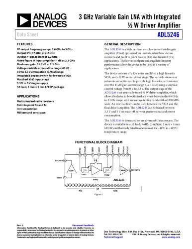
 ADL5246
32 ページ
-
 ADA4961
22 ページ
-
 AN-1141
8 ページ
-
 AN-698
36 ページ
-
 Temperature Sensors
2 ページ
-
 Reference Circuits
8 ページ
-
 Precision ADCs
16 ページ