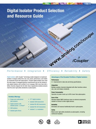
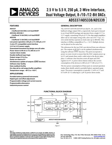
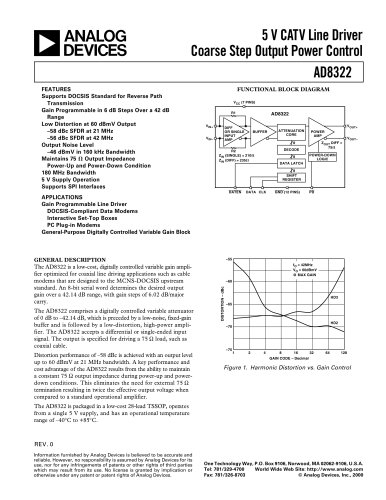
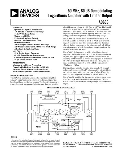
カタログの抜粋
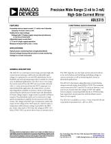
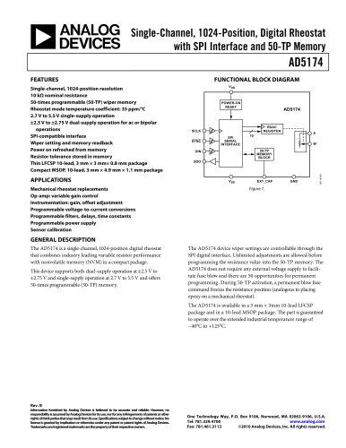
Precision Wide Range (3 nA to 3 mA) High-Side Current Mirror ADL5315 FEATURES Accurately mirrors input current (1:1 ratio) over 6 decades Linearity 1% from 3 nA to 3 mA Stable mirror input voltage Voltage held 1 V below supply using internal reference or can be set externally Adjustable input current limit 2.7 V to 8 V single-supply operation Miniature 8-lead LFCSP (2 mm × 3 mm) FUNCTIONAL BLOCK DIAGRAM ADL5315 VOLTAGE REFERENCE 4 CURRENT LIMITING RLIM CURRENT MIRROR 1:1 APPLICATIONS IOUT Optical power monitoring from a single photodiode General voltage biasing with precision current monitoring Voltage-to-current conversion GENERAL DESCRIPTION The ADL5315 is a wide input current range, precision high-side current mirror featuring a stable and user-adjustable input voltage. It is optimized for use with PIN photodiodes, but its flexibility and wide operating range make it suitable for a broad array of additional applications. Over the 3 nA to 3 mA range, the current sourced from the INPT pin is accurately mirrored with a 1:1 ratio and sourced from the IOUT output pin. In a typical photodiode application, the output drives a currentinput logarithmic amplifier to produce a linear-in-dB output representing the optical power incident upon the photodiode. For linear voltage output, a single resistor to ground is all that is required. The photodiode anode can be connected to a high speed transimpedance amplifier for the extraction of the data stream. The voltage at the INPT pin is temperature stable with respect to the voltage at the VSET input pin, which it tracks. A temperature stable reference voltage is provided at the SREF pin, which, when tied to VSET, fixes the voltage at INPT 1.0 V below VPOS. VSET can also be driven from an external source. The VSET input has very low input current and can be driven as low as the bottom rail, facilitating nonloading voltage-tocurrent conversion as well as minimizing dark current in photodiode applications. The ADL5315 also features adjustable input current limiting using an external resistor from RLIM to VPOS. The maximum current sourced by INPT (and IOUT) can be set between 1 mA and 16 mA, beyond which the voltage at INPT falls rapidly from its setpoint. Connecting RLIM directly to VPOS provides basic input short-circuit protection with the default current limit of 16 mA typical. The ADL5315 is available in a 2 mm × 3 mm, 8-lead LFCSP and is specified for operation from −40°C to +85°C. Rev. 0 Information furnished by Analog Devices is believed to be accurate and reliable. However, no responsibility is assumed by Analog Devices for its use, nor for any infringements of patents or other rights of third parties that may result from its use. Specifications subject to change without notice. No license is granted by implication or otherwise under any patent or patent rights of Analog Devices. Trademarks and registered trademarks are the property of their respective owners. One Technology Way, P.O. Box 9106, Norwood, MA 02062-9106, U.S.A. Tel: 781.329.4700 www.analog.com Fax: 781.461.3113 © 2005 Analog Devices, Inc. All rights reserved.
カタログの1ページ目を開く
REVISION HISTORY 10/05—Revision 0: Initial Version
カタログの2ページ目を開く
ADL5315 SPECIFICATIONS VPOS = 5 V, VSET = 4 V, IINPT = 3 μA, TA = 25°C, unless otherwise noted. Table 1. Parameter CURRENT MIRROR OUTPUT Current Gain from INPT to IOUT Current Gain from INPT to IOUT Nonlinearity Small Signal Bandwidth Wideband Noise at IPDM Specified Output Voltage Range IOUT × ROUT Product MIRROR INPUT, VOLTAGE CONTROL Specified Input Current Range, IINPT Specified VSET Voltage Range Incremental Gain from VSET to INPT Incremental Input Resistance at VSET Input Bias Current at VSET SREF Voltage, Relative to VPOS OVERCURRENT PROTECTION INPT Current Limit POWER SUPPLY Supply...
カタログの3ページ目を開く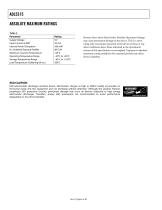
ADL5315 ABSOLUTE MAXIMUM RATINGS Table 2. Parameter Supply Voltage Input Current at INPT Internal Power Dissipation θJA (Soldered Exposed Paddle) Maximum Junction Temperature Operating Temperature Range Storage Temperature Range Lead Temperature (Soldering 60 sec) Stresses above those listed under Absolute Maximum Ratings may cause permanent damage to the device. This is a stress rating only; functional operation of the device at these or any other conditions above those indicated in the operational section of this specification is not implied. Exposure to absolute maximum rating conditions...
カタログの4ページ目を開く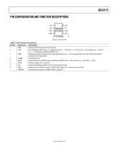
ADL5315 PIN CONFIGURATION AND FUNCTION DESCRIPTIONS 8 IOUT Table 3. Pin Function Descriptions Pin No. 1 2 Mnemonic INPT VSET COMM RLIM VPOS N/C IOUT PADDLE Description Input Current. Pin sources current only. Sets Voltage at INPT (Gain = 1). Range 0 V to VPOS − 1.0 V for VPOS < 6.5 V. For VPOS ≥ 6.5 V range, VPOS − 6.5 V to VPOS − 1 V. Optional shielding of INPT trace. Reference Voltage for VSET. Internally generated at VPOS − 1.0 V through 20 kΩ. Can be shorted to VSET for standard mirror operation. Analog Ground. External Resistor to VPOS. Sets current limit at INPT from 1 mA to 16 mA....
カタログの5ページ目を開く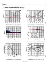
ADL5315 TYPICAL PERFORMANCE CHARACTERISTICS VPOS = 5 V, VSET = VSREF, VOUT = 0 V, TA = 25°C, unless otherwise noted. 2.0 1.5 VPOS = 2.7V, VSET = VSREF VPOS = 5V, VSET = 2V VPOS = 5V, VSET = VSREF VPOS = 8V, VSET = 2V VPOS = 8V, VSET = VSREF IINPT VS. IOUT, ALL VOLTAGE CONDITIONS Figure 3. IOUT Linearity vs. IINPT for Multiple Temperatures, Normalized to 25°C and IINPT = 3 μA Figure 6. IOUT Linearity vs. IINPT for Multiple Supply Conditions, Normalized to VPOS = 5 V, VSET = VSREF, and IINPT = 3 μA –20 –40 –40°C, VPOS = 2.7V, VSET = VSREF –40°C, VPOS = 5V, VSET = 0V –40°C, VPOS = 5V, VSET =...
カタログの6ページ目を開く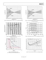
Figure 9. Temperature Drift of VINPT with VSET = VSREF, 3-σ to Either Side of Mean Figure 12. Temperature Drift of VINPT with VSET = 4 V (External Voltage Source), 3-σ to Either Side of Mean 10m Figure 13. Pulse Response of IINPT to IOUT for IOUT in Decades from 3 nA to 3 mA Figure 10. Small-Signal AC Response of IINPT to IOUT for IINPT in Decades from 3 nA to 3 mA 4.5 Figure 11. Pulse Response of VSET to VINPT (VSET Pulsed from 0 V to 4 V) for Multiple Values of IINPT VPOS = 2.7V, VSET = VSREF 6 VPOS = 5V, VSET = VSREF ERROR FROM CALCULATED CURRENT LIMIT (%) Figure 14. Current Limit Error...
カタログの7ページ目を開くAnalog Devices/アナログ・デバイセズのすべてのカタログと技術パンフレット
-
 HMC722LP3E
8 ページ
-
 HMC853 Data Sheet
10 ページ
-
 AN-1084
8 ページ
-
 AN-1091
2 ページ
-
 AN_737
8 ページ
-
 AN-0982
4 ページ
-
 ADF7024
24 ページ
-
 AD9915
48 ページ
-
 AD9914
48 ページ
-
 ADRF6612
59 ページ
-
 ADRF6820
48 ページ
-
 ADL5246
32 ページ
-
 ADA4961
22 ページ
-
 AN-1141
8 ページ
-
 AN-698
36 ページ
-
 Temperature Sensors
2 ページ
-
 Reference Circuits
8 ページ
-
 Precision ADCs
16 ページ