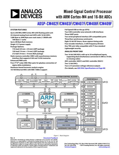
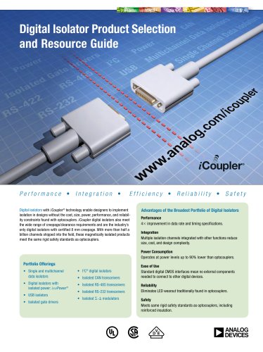
カタログの抜粋
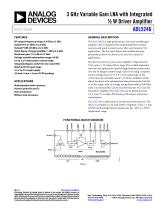
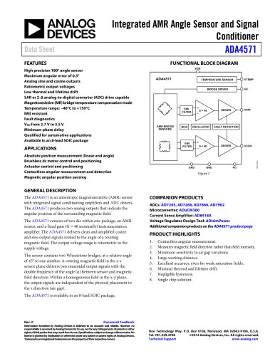
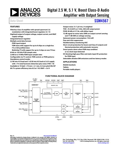
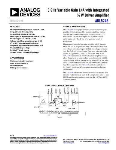
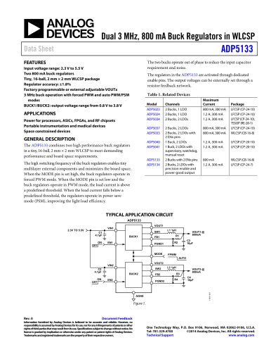
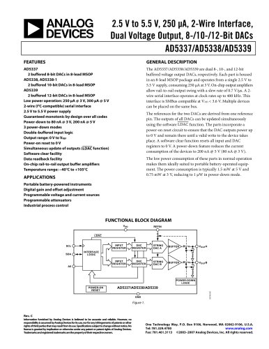
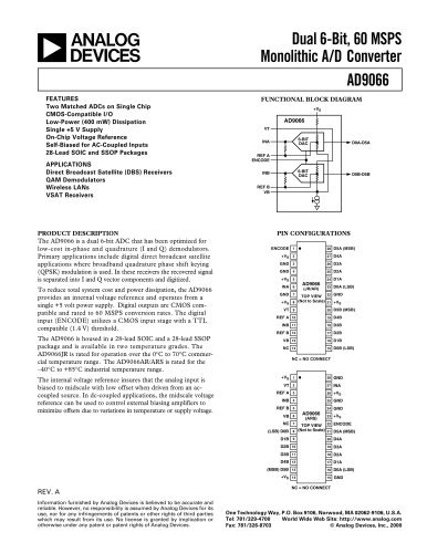
3 GHz Variable Gain LNA with Integrated ½ W Driver Amplifier ADL5246 Data Sheet FEATURES GENERAL DESCRIPTION RF output frequency range: 0.6 GHz to 3 GHz Output IP3: 37 dBm at 2.2 GHz Output P1dB: 28 dBm at 2.2 GHz Noise figure of input amplifier: 1 dB at 2.2 GHz Maximum gain: 31.5 dB at 2.2 GHz Voltage variable attenuation range: 45 dB 0 V to 3.3 V attenuation control range Integrated bypass switch for low noise VGA Matched 50 Ω input stage 3.3 V to 5 V single supply 32-lead, 5 mm × 5 mm LFCSP package The ADL5246 is a high performance, low noise variable gain amplifier (VGA) optimized for multistandard base station receivers and point to point receive (Rx) and transmit (Tx) applications. The low noise figure and excellent linearity performance allow the device to be used in a variety of applications. The device consists of a low noise amplifier, a high linearity VGA, and a ½ W output driver stage. The variable attenuator networks are optimized to provide high linearity performance over the 45 dB gain control range. Gain is set using a unipolar control voltage from 0 V to 3.3 V. The output stage of the ADL5246 is an externally tuned ½ W driver amplifier, which allows the device to be optimized anywhere between the 0.6 GHz to 3 GHz range, with an average tuning bandwidth of 200 MHz wide. An external filter can be used between the VGA and the final driver amplifier. The ADL5246 can be biased between 3.3 V and 5 V to trade-off between performance and power consumption. APPLICATIONS Multistandard radio receivers Point to point Rx and Tx Instrumentation Military and aerospace The ADL5246 is fabricated on an advanced GaAs process. The device is available in a 32-lead, RoHS-compliant, 5 mm × 5 mm LFCSP and thermally rated to operate over the −40°C to +105°C temperature range. FUNCTIONAL BLOCK DIAGRAM Document Feedback Information furnished by Analog Devices is believed to be accurate and reliable. However, no responsibility is assumed by Analog Devices for its use, nor for any infringements of patents or other rights of third parties that may result from its use. Specifications subject to change without notice. No license is granted by implication or otherwise under any patent or patent rights of Analog Devices. Trademarks and registered trademarks are the property of their respective owners. One Technology Way, P.O. Box 9106, Norwood, MA 02062-9106, U.S.A. Tel: 781.329.4700 ©2014 Analog Devices, Inc. All rights reserved. Technical Support www.analog.com
カタログの1ページ目を開く
Data Sheet REVISION HISTORY 4/14—Revision 0: Initial Version
カタログの2ページ目を開く
Data Sheet SPECIFICATIONS VPOS = 5 V, TA = 25°C, unless otherwise noted. Amplifier 1 = AMP1, Amplifier 2 = AMP2, and Amplifier 3 = AMP3. Table 1. Parameter OVERALL FUNCTION Frequency Range AMP1 FREQUENCY = 0.75 GHz Gain vs. Frequency vs. Temperature vs. Supply Input Return Loss Output Return Loss Output 1 dB Compression Point Output Third-Order Intercept Noise Figure AMP1 FREQUENCY = 0.9 GHz Gain vs. Frequency vs. Temperature vs. Supply Input Return Loss Output Return Loss Output 1 dB Compression Point Output Third-Order Intercept Noise Figure AMP1 FREQUENCY = 1.5 GHz Gain vs. Frequency vs....
カタログの3ページ目を開く
ADL5246 Parameter AMP1 FREQUENCY = 2.2 GHz Gain vs. Frequency vs. Temperature vs. Supply Input Return Loss Output Return Loss Output 1 dB Compression Point Output Third-Order Intercept Noise Figure AMP1 FREQUENCY = 2.6 GHz Gain vs. Frequency vs. Temperature vs. Supply Input Return Loss Output Return Loss Output 1 dB Compression Point Output Third-Order Intercept Noise Figure AMP2 FREQUENCY = 0.75 GHz Gain vs. Frequency vs. Temperature Gain Range Input Return Loss Output Return Loss Input 1 dB Compression Point Input Third-Order Intercept Noise Figure AMP2 FREQUENCY = 0.9 GHz Gain vs....
カタログの4ページ目を開く
Data Sheet Parameter AMP2 FREQUENCY = 1.9 GHz Gain vs. Frequency vs. Temperature Gain Range Input Return Loss Output Return Loss Input 1 dB Compression Point Input Third-Order Intercept Noise Figure AMP2 FREQUENCY = 2.2 GHz Gain vs. Frequency vs. Temperature Gain Range Input Return Loss Output Return Loss Input 1 dB Compression Point Input Third-Order Intercept Noise Figure AMP2 FREQUENCY = 2.6 GHz Gain vs. Frequency vs. Temperature Gain Range Input Return Loss Output Return Loss Input 1 dB Compression Point Input Third-Order Intercept Noise Figure AMP2 GAIN SETTLING Minimum to Maximum Gain...
カタログの5ページ目を開く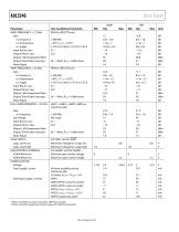
ADL5246 Parameter AMP3 FREQUENCY = 2.2 GHz Gain vs. Frequency vs. Temperature vs. Supply Input Return Loss Output Return Loss Output 1 dB Compression Point Output Third-Order Intercept Noise Figure AMP3 FREQUENCY = 2.6 GHz Gain vs. Frequency vs. Temperature vs. Supply Input Return Loss Output Return Loss Output 1 dB Compression Point Output Third-Order Intercept Noise Figure FULL CHAIN FREQUENCY = 2.2 GHz Gain vs. Frequency Gain Range Input Return Loss Output Return Loss Output 1 dB Compression Point Output Third-Order Intercept Noise Figure LOGIC INPUTS Logic Level Low Logic Level High...
カタログの6ページ目を開く
Data Sheet ABSOLUTE MAXIMUM RATINGS Supply Voltage, Vpos Maximum RF Input Level (AMP1) Internal Power Dissipation Maximum Junction Temperature Operating Temperature Range Storage Temperature Range Lead Temperature Range (Soldering 30 sec) Human Body Model (HBM) ESD Rating Stresses at or above those listed under Absolute Maximum Ratings may cause permanent damage to the product. This is a stress rating only; functional operation of the product at these or any other conditions above those indicated in the operational section of this specification is not implied. Operation beyond the maximum...
カタログの7ページ目を開く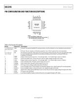
Data Sheet PIN CONFIGURATION AND FUNCTION DESCRIPTIONS NOTES 1. NIC = NO INTERNAL CONNECTION. 2. THE EXPOSED PADDLE (EP) MUST BE SOLDERED TO A LOW IMPEDANCE GROUND PLANE. Description Ground. The exposed paddle (EP) and ground pins must be soldered to a low impedance ground plane. RF Input. This pin requires a dc blocking capacitor. Use a 100 pF capacitor for normal operation. No Internal Connection. These pins are not connected to internal circuitry. The user may optionally solder to a low impedance ground plane for grounding, shielding, and printed circuit board (PCB) trace impedance...
カタログの8ページ目を開くAnalog Devices/アナログ・デバイセズのすべてのカタログと技術パンフレット
-
 HMC722LP3E
8 ページ
-
 HMC853 Data Sheet
10 ページ
-
 AN-1084
8 ページ
-
 AN-1091
2 ページ
-
 AN_737
8 ページ
-
 AN-0982
4 ページ
-
 ADF7024
24 ページ
-
 AD9915
48 ページ
-
 AD9914
48 ページ
-
 ADRF6612
59 ページ
-
 ADRF6820
48 ページ
-
 ADA4961
22 ページ
-
 AN-1141
8 ページ
-
 AN-698
36 ページ
-
 Temperature Sensors
2 ページ
-
 Reference Circuits
8 ページ
-
 Precision ADCs
16 ページ