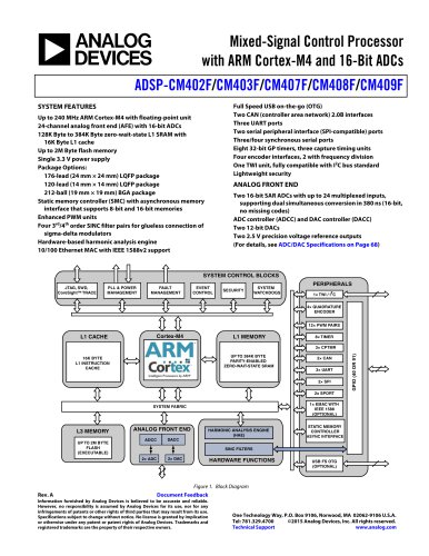
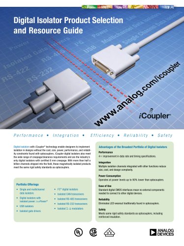
カタログの抜粋
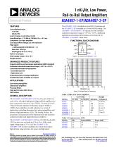
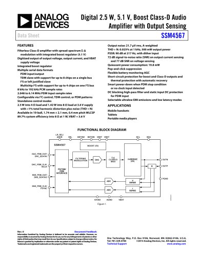
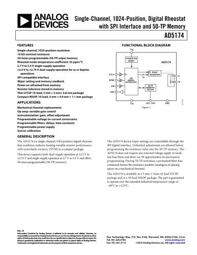
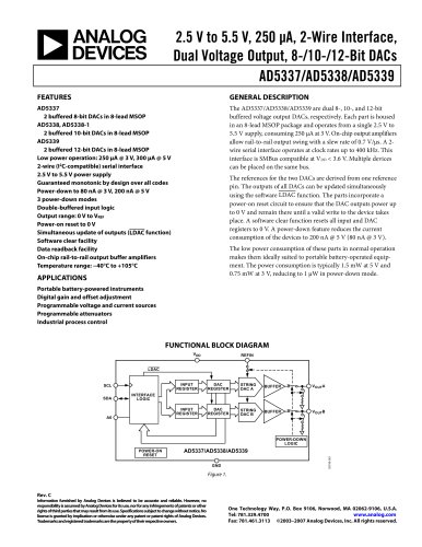
1 nV/√Hz, Low Power, Rail-to-Rail Output Amplifiers ADA4897-1-EP/ADA4897-2-EP FEATURES Low wideband noise 1 nV/√Hz 2.8 pA/√Hz Low 1/f noise: 2.4 nV/√Hz at 10 Hz Low distortion: −115 dBc at 100 kHz, VOUT = 2 V p-p Low power: 3 mA per amplifier Low input offset voltage: 0.5 mV maximum High speed −3 dB bandwidth: 230 MHz (G = +1) Slew rate: 120 V/μs Settling time to 0.1%: 45 ns Rail-to-rail output Wide supply range: 3 V to 10 V Disable feature The ADA4897-1-EP is available in 6-lead SOT-23 package and the ADA4897-2-EP is available in a 10-lead MSOP package. The ADA4897-1-EP/ADA4897-2-EP operate over the extended industrial temperature range of −55°C to +125°C. Additional application and technical information can be found in the ADA4897-1/ADA4897-2 data sheet. FUNCTIONAL BLOCK DIAGRAM ADA4897-1-EP OUT 1 ENHANCED PRODUCT FEATURES VOLTAGE NOISE (nV/√Hz) Supports defense and aerospace applications (AQEC standard) Extended industrial temperature range (−55°C to +125°C) Controlled manufacturing baseline 1 assembly/test site 1 fabrication site Enhanced product change notification Qualification data available on request Low noise preamplifier Ultrasound amplifiers PLL loop filters High performance ADC drivers DAC buffers Figure 2. Voltage Noise vs. Frequency Table 1. Other Low Noise Amplifiers GENERAL DESCRIPTION The ADA4897-1-EP/ADA4897-2-EP are unity-gain stable, low noise, rail-to-rail output, high speed voltage feedback amplifiers that have a quiescent current of 3 mA. With a 1/f noise of 2.4 nV/ √Hz at 10 Hz and a spurious-free dynamic range of −80 dBc at 2 MHz, these amplifiers are ideal solutions in a variety of applications, including ultrasound, low noise preamplifiers, and drivers of high performance ADCs. The Analog Devices, Inc., proprietary next-generation SiGe bipolar process and innovative architecture enable such high performance amplifiers. The ADA4897-1-EP/ADA4897-2-EP have 230 MHz bandwidth, 120 V/μs slew rate, and settle to 0.1% in 45 ns. With a wide supply voltage range of 3 V to 10 V, the ADA4897-1-EP/ ADA4897-2-EP are ideal candidates for systems that require high dynamic range, precision, low power, and high speed. Enhanced Product Table 2. Complementary ADCs Bits 14 16 18 Document Feedback Information furnished by Analog Devices is believed to be accurate and reliable. However, no responsibility is assumed by Analog Devices for its use, nor for any infringements of patents or other rights of third parties that may result from its use. Specifications subject to change without notice. No license is granted by implication or otherwise under any patent or patent rights of Analog Devices. Trademarks and registered trademarks are the property of their respective owners. One Technology Way, P.O. Box 9106, Norwood, MA 02062-9106, U.S.A. Tel: 781.329.4700 ©2013 Analog Devices, Inc. All rights reserved. Technical Support www.analog.com
カタログの1ページ目を開く
Enhanced Product REVISION HISTORY 2/13—Revision 0: Initial Version
カタログの2ページ目を開く
Enhanced Product SPECIFICATIONS ±5 V SUPPLY TA = 25°C, G = +1, RL = 1 kΩ to ground, unless otherwise noted. Table 3. Parameter DYNAMIC PERFORMANCE −3 dB Bandwidth Bandwidth for 0.1 dB Flatness Slew Rate Settling Time to 0.1% Settling Time to 0.01% NOISE/HARMONIC PERFORMANCE Harmonic Distortion (SFDR) Input Voltage Noise Input Current Noise 0.1 Hz to 10 Hz Noise DC PERFORMANCE Input Offset Voltage Input Offset Voltage Drift Input Bias Current Input Bias Current Drift Input Bias Offset Current Open-Loop Gain INPUT CHARACTERISTICS Input Resistance Common-Mode Differential Input Capacitance...
カタログの3ページ目を開く
ADA4897-1-EP/ADA4897-2-EP Parameter POWER SUPPLY Operating Range Quiescent Current per Amplifier Enhanced Product Test Conditions/Comments Enabled Disabled DISABLE = −5 V Power Supply Rejection Ratio (PSRR) Positive Negative DISABLE PIN DISABLE Voltage Input Current Enabled Disabled Switching Speed Enabled Disabled +5 V SUPPLY TA = 25°C, G = +1, RL = 1 kΩ to midsupply, unless otherwise noted. Table 4. Parameter DYNAMIC PERFORMANCE −3 dB Bandwidth Bandwidth for 0.1 dB Flatness Slew Rate Settling Time to 0.1% Settling Time to 0.01% NOISE/HARMONIC PERFORMANCE Harmonic Distortion (SFDR) Input...
カタログの4ページ目を開く
Enhanced Product Parameter INPUT CHARACTERISTICS Input Resistance Common-Mode Differential Input Capacitance Common-Mode Differential Input Common-Mode Voltage Range Common-Mode Rejection Ratio (CMRR) OUTPUT CHARACTERISTICS Output Overdrive Recovery Time Output Voltage Swing Positive Negative Output Current Short-Circuit Current Capacitive Load Drive POWER SUPPLY Operating Range Quiescent Current per Amplifier Input Current Enabled Disabled Switching Speed Enabled Disabled Enabled Disabled VIN = 0 V to 5 V, G = +2 RL = 1 kΩ RL = 100 Ω RL = 1 kΩ RL = 100 Ω SFDR = −45 dBc Sinking/sourcing 30%...
カタログの5ページ目を開く
Enhanced Product +3 V SUPPLY TA = 25°C, G = +1, RL = 1 kΩ to midsupply, unless otherwise noted. Table 5. Parameter DYNAMIC PERFORMANCE −3 dB Bandwidth Bandwidth for 0.1 dB Flatness Slew Rate Settling Time to 0.1% Settling Time to 0.01% NOISE/HARMONIC PERFORMANCE Harmonic Distortion (SFDR) Input Voltage Noise Input Current Noise 0.1 Hz to 10 Hz Noise DC PERFORMANCE Input Offset Voltage Input Offset Voltage Drift Input Bias Current Input Bias Current Drift Input Bias Offset Current Open-Loop Gain INPUT CHARACTERISTICS Input Resistance Common-Mode Differential Input Capacitance Common-Mode...
カタログの6ページ目を開く
Enhanced Product Parameter POWER SUPPLY Operating Range Quiescent Current per Amplifier Enabled Disabled DISABLE = 0 V Power Supply Rejection Ratio (PSRR) Positive Negative DISABLE PIN DISABLE Voltage Input Current Enabled Disabled Switching Speed Enabled Disabled
カタログの7ページ目を開く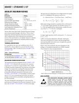
Enhanced Product ABSOLUTE MAXIMUM RATINGS Table 6. Rating 11 V See Figure 3 −VS − 0.7 V to +VS + 0.7 V 0.7 V −65°C to +125°C −55°C to +125°C 300°C 150°C Stresses above those listed under Absolute Maximum Ratings may cause permanent damage to the device. This is a stress rating only; functional operation of the device at these or any other conditions above those indicated in the operational section of this specification is not implied. Exposure to absolute maximum rating conditions for extended periods may affect device reliability. THERMAL RESISTANCE θJA is specified for the worst-case...
カタログの8ページ目を開くAnalog Devices/アナログ・デバイセズのすべてのカタログと技術パンフレット
-
 HMC722LP3E
8 ページ
-
 HMC853 Data Sheet
10 ページ
-
 AN-1084
8 ページ
-
 AN-1091
2 ページ
-
 AN_737
8 ページ
-
 AN-0982
4 ページ
-
 ADF7024
24 ページ
-
 AD9915
48 ページ
-
 AD9914
48 ページ
-
 ADRF6612
59 ページ
-
 ADRF6820
48 ページ
-
 ADL5246
32 ページ
-
 ADA4961
22 ページ
-
 AN-1141
8 ページ
-
 AN-698
36 ページ
-
 Temperature Sensors
2 ページ
-
 Reference Circuits
8 ページ
-
 Precision ADCs
16 ページ