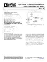
AD5174: Single-Channel, 1024-Position, Digital Rheostat with SPI interface and 50-TP Memory
1 /
20ページ

カタログの抜粋
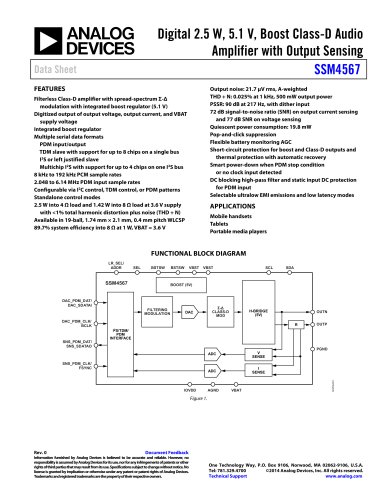
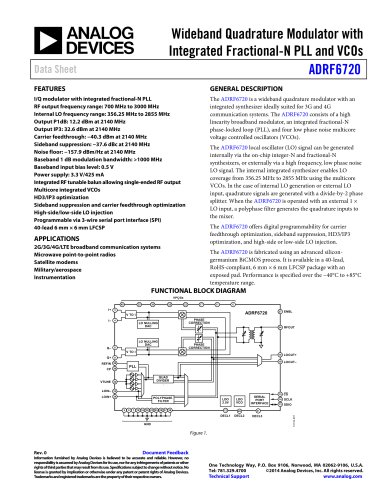
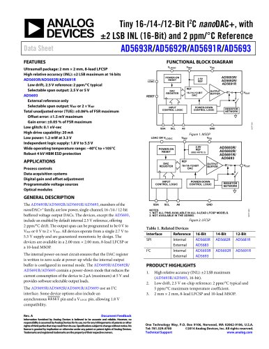
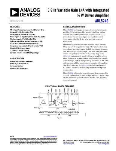
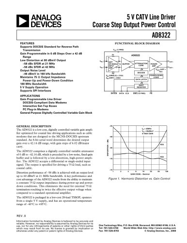
Single-Channel, 1024-Position, Digital Rheostat with SPI Interface and 50-TP Memory AD5174 Rev. B Information furnished by Analog Devices is believed to be accurate and reliable. However, no responsibility is assumed by Analog Devices for its use, nor for any infringements of patents or other rights of third parties that may result from its use. Specifications subject to change without notice. No license is granted by implication or otherwise under any patent or patent rights of Analog Devices. Trademarks and registered trademarks are the property of their respective owners. One Technology Way, P.O. Box 9106, Norwood, MA 02062-9106, U.S.A. Tel: 781.329.4700 www.analog.com Fax: 781.461.3113 ©2010 Analog Devices, Inc. All rights reserved. FEATURES Single-channel, 1024-position resolution 10 kÙ nominal resistance 50-times programmable (50-TP) wiper memory Rheostat mode temperature coefficient: 35 ppm/°C 2.7 V to 5.5 V single-supply operation ±2.5 V to ±2.75 V dual-supply operation for ac or bipolar operations SPI-compatible interface Wiper setting and memory readback Power on refreshed from memory Resistor tolerance stored in memory Thin LFCSP 10-lead, 3 mm × 3 mm× 0.8 mm package Compact MSOP, 10-lead, 3 mm × 4.9 mm × 1.1 mm package APPLICATIONS Mechanical rheostat replacements Op-amp: variable gain control Instrumentation: gain, offset adjustment Programmable voltage-to-current conversions Programmable filters, delays, time constants Programmable power supply Sensor calibration FUNCTIONAL BLOCK DIAGRAM 10VDDVSSEXT_CAPGNDAWAD5174SCLKDINSDOSPISERIALINTERFACEPOWER-ONRESETRDACREGISTER50-TPMEMORYBLOCKSYNC08718-001 Figure 1. GENERAL DESCRIPTION The AD5174 is a single-channel, 1024-position digital rheostat that combines industry leading variable resistor performance with nonvolatile memory (NVM) in a compact package. This device supports both dual-supply operation at ±2.5 V to ±2.75 V and single-supply operation at 2.7 V to 5.5 V and offers 50-times programmable (50-TP) memory. The AD5174 device wiper settings are controllable through the SPI digital interface. Unlimited adjustments are allowed before programming the resistance value into the 50-TP memory. The AD5174 does not require any external voltage supply to facili-tate fuse blow and there are 50 opportunities for permanent programming. During 50-TP activation, a permanent blow fuse command freezes the resistance position (analogous to placing epoxy on a mechanical rheostat). The AD5174 is available in a 3 mm × 3mm 10-lead LFCSP package and in a 10-lead MSOP package. The part is guaranteed to operate over the extended industrial temperature range of -40°C to +125°C.
カタログの1ページ目を開く
AD5174 Rev. B | Page 3 of 20 SPECIFICATIONS ELECTRICAL CHARACTERISTICS VDD = 2.7 V to 5.5 V, VSS = 0 V; VDD = 2.5 V to 2.75 V, VSS = -2.5 V to -2.75 V; -40°C < TA < 125°C, unless otherwise noted. Table 1. Parameter Symbol Test Conditions/Comments Min Typ1 Max Unit DC CHARACTERISTICS—RHEOSTAT MODE Resolution 10 Bits Resistor Integral Nonlinearity2, 3 R-INL |VDD - VSS| = 3.6 V to 5.5 V -1 +1 LSB |VDD - VSS| = 3.3 V to 3.6 V -1 +1.5 LSB |VDD - VSS| = 2.7 V to 3.3 V -2.5 +2.5 LSB Resistor Differential Nonlinearity2 R-DNL -1 +1 LSB Nominal Resistor Tolerance ±15 % Resistance Temperature...
カタログの3ページ目を開く
AD5174 Rev. B | Page 4 of 20 Parameter Symbol Test Conditions/Comments Min Typ1 Max Unit DYNAMIC CHARACTERISTICS4, 10 Bandwidth -3 dB, RAW = 5 kÙ, Terminal W, see Figure 24 700 kHz Total Harmonic Distortion VA = 1 V rms, f = 1 kHz, RAW = 5 kÙ -90 dB Resistor Noise Density RWB = 5 kÙ, TA = 25°C, f = 10 kHz 13 nV/ãHz 1 Typical specifications represent average readings at 25°C, VDD = 5 V, and VSS = 0 V. 2 Resistor position nonlinearity error (R-INL) is the deviation from an ideal value measured between the maximum resistance and the minimum resistance wiper positions. R-DNL measures the...
カタログの4ページ目を開く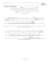
AD5174 Rev. B | Page 5 of 20 Shift Register and Timing Diagrams DATA BITSDB9 (MSB)DB0 (LSB)D7D6D5D4D3D2D1D0CONTROL BITSC0C1C2 D9D8C30008718-002 Figure 2. Shift Register Content 00C3C2D7D6D5D2D1D0SCLKSDODINSYNCt7t9t1t2t4t3t8t5t608718-003 Figure 3. Write Timing Diagram, CPOL=0, CPHA = 1 t10t90000C3C3XXC3D1D0D1D0D0D0SCLKSDODINSYNC08718-004 Figure 4. Read Timing Diagram, CPOL=0, CPHA = 1
カタログの5ページ目を開く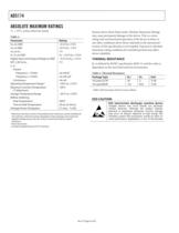
AD5174 Rev. B | Page 6 of 20 ABSOLUTE MAXIMUM RATINGS TA = 25°C, unless otherwise noted. Table 3. Parameter Rating VDD to GND –0.3 V to +7.0 V VSS to GND +0.3 V to -7.0 V VDD to VSS 7 V VA, VW to GND VSS - 0.3 V, VDD + 0.3 V Digital Input and Output Voltage to GND -0.3 V to VDD + 0.3 V EXT_CAP to VSS 7 V IA, IW Pulsed1 Frequency > 10 kHz ±6 mA/d2 Frequency 10 kHz ±6 mA/ãd2 Continuous ±6 mA Operating Temperature Range3 -40°C to +125°C Maximum Junction Temperature (TJ Maximum) 150°C Storage Temperature Range -65°C to +150°C Reflow Soldering Peak Temperature 260°C Time at Peak Temperature 20...
カタログの6ページ目を開く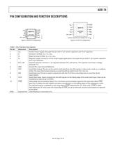
AD5174 Rev. B | Page 7 of 20 PIN CONFIGURATION AND FUNCTION DESCRIPTIONS VDD11VSS22A33W44SDO1098SCLK75EXT_CAPDIN6GNDAD5174TOP VIEW(Not toScale)SYNC08718-005 SYNCVDD1VSS2A3W4SDO1098SCLK75EXT_CAPDIN6GND*LEAVE FLOATING OR CONNECTED TO VSS.AD5174(EXPOSEDPAD)*08718-103 Figure 5. MSOP Pin Configuration Figure 6. LFCSP Pin Configuration Table 5. Pin Function Descriptions Pin No. Mnemonic Description 1 VDD Positive Power Supply. Decouple this pin with 0.1 ìF ceramic capacitors and 10 ìF capacitors. 2 A Terminal A of RDAC. VSS VA VDD. 3 W Wiper Terminal of RDAC. VSS VW VDD. 4 VSS Negative Supply....
カタログの7ページ目を開く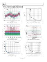
AD5174 Rev. B | Page 8 of 20 TYPICAL PERFORMANCE CHARACTERISTICS 0.8–0.6–0.4–0.200.20.40.601282563845126407688961023INL ( LSB)CODE (Decimal)08718-014+25°C–40°C+125°C Figure 7. R-INL vs. Code vs. Temperature 0.4–0.3–0.2–0.100.10.20.301282563845126407688961023DNL ( LSB)CODE (Decimal)08718-015+25°C–40°C+125°C Figure 8. R-DNL vs. Code vs. Temperature 700600500400300200100001282563845126407688961023RHEOSTAT MODE TEMPCO ( ppm/°C)CODE (Decimal)08718-019VDD/VSS = 5V/0V Figure 9. Tempco ÄRWA/ÄT vs. Code 00.20.40.60.81.0CURRENT ( mA)VOLTAGE (V)00.51.01.52.02.53.03.54.04.55.05.508718-023VDD/VSS =...
カタログの8ページ目を開くAnalog Devices/アナログ・デバイセズのすべてのカタログと技術パンフレット
-
 HMC722LP3E
8 ページ
-
 HMC853 Data Sheet
10 ページ
-
 AN-1084
8 ページ
-
 AN-1091
2 ページ
-
 AN_737
8 ページ
-
 AN-0982
4 ページ
-
 ADF7024
24 ページ
-
 AD9915
48 ページ
-
 AD9914
48 ページ
-
 ADRF6612
59 ページ
-
 ADRF6820
48 ページ
-
 ADL5246
32 ページ
-
 ADA4961
22 ページ
-
 AN-1141
8 ページ
-
 AN-698
36 ページ
-
 Temperature Sensors
2 ページ
-
 Reference Circuits
8 ページ
-
 Precision ADCs
16 ページ