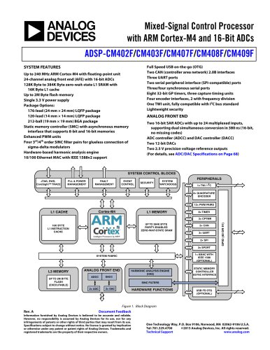
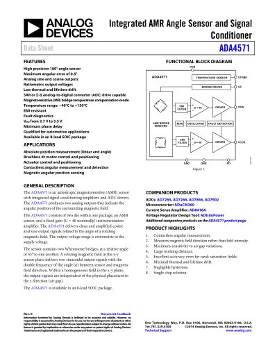
A 16-Bit, 6 MSPS SAR ADC System with Low Power Input Drivers and Reference Optimized for Multiplexed Applications
1 /
5ページ

カタログの抜粋
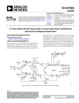
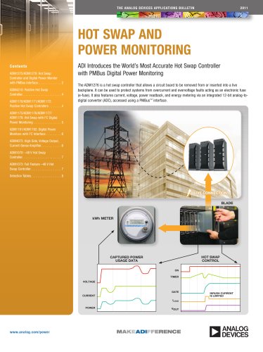
Circuit Note Circuits from the Lab™ reference circuits are engineered and tested for quick and easy system integration to help solve today’s analog, mixed-signal, and RF design challenges. For more information and/or support, visit www.analog.com/CN0307. 16-Bit, 6 MSPS, PulSAR, Differential ADC Low Power, Low Noise, Single/Dual Amplifier Ultralow Noise XFET Voltage Reference with Current Sink and Source Capability 2.7 V, 800 µA, 80 MHz Single/Dual Rail-toRail I/O Amplifier A 16-Bit, 6 MSPS SAR ADC System with Low Power Input Drivers and Reference Optimized for Multiplexed Applications EVALUATION AND DESIGN SUPPORT distortion [THD] = −110 dBc) at low power. The circuit is ideal for high performance multiplexed data acquisition systems, such as portable digital x-ray systems and security scanners, because the SAR architecture can sample without the latency or pipeline delay typically incurred with pipeline ADCs. The 6 MSPS sampling rate allows fast sampling of multiple channels, and the ADC has true 16-bit dc linearity performance and a serial low voltage differential signaling (LVDS) interface for low pin count and low digital noise. Design and Integration Files Schematics, Layout Files, Bill of Materials CIRCUIT FUNCTION AND BENEFITS The circuit in Figure 1 is a 16-bit, 6 MSPS, successive approximation (SAR) analog-to-digital converter (ADC) and differential-todifferential driver combination optimized for low noise (signal-tonoise ratio [SNR] = 88.6 dB) and low distortion (total harmonic Figure 1. The ADA4897-1 Driving the AD7625 (All Connections and Decoupling Not Shown) Rev. 0 Circuits from the Lab™ circuits from Analog Devices have been designed and built by Analog Devices engineers. Standard engineering practices have been employed in the design and construction of each circuit, and their function and performance have been tested and verified in a lab environment at room temperature. However, you are solely responsible for testing the circuit and determining its suitability and applicability for your use and application. Accordingly, in no event shall Analog Devices be liable for direct, indirect, special, incidental, consequential or punitive damages due to any cause whatsoever connected to the use of any Circuits from the Lab circuits. (Continued on last page) One Technology Way, P.O. Box 9106, Norwood, MA 02062-9106, U.S.A. Tel: 781.329.4700 www.analog.com Fax: 781.461.3113 ©2012 Analog Devices, Inc. All rights reserved.
カタログの1ページ目を開く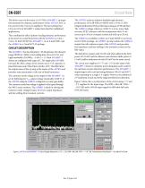
Circuit Note The driver uses two low noise (1 nV/VHz) ADA4897-1 op amps that maintain the dynamic performance of the AD7625 ADC at low power levels (3 mA per amplifier). The fast settling time (45 ns to 0.1%) of ADA4897-1 makes them ideal for multiplexed This combination offers industry-leading dynamic performance at low power in a small board area with the AD7625 in a 5 mm x CIRCUIT DESCRIPTION The ADA4897-1 has low distortion (-93 dB spurious-free dynamic range [SFDR] at 1 MHz), a fast settling time (36 ns to 0.1%), and high bandwidth (230 MHz, -3 dB, G = 1). Both ADA4897-1 drivers are...
カタログの2ページ目を開く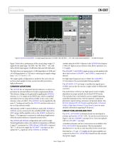
Circuit Note Figure 3. AD7625 and ADA4897-1 in Single Supply Operation (5 V), SNR = 86.7 dB, THD = −101.1 dB, Fundamental Amplitude = −1.55 dB of Full Scale Figure 3 shows the ac performance of the circuit using a single 5 V supply for the input stage. The SNR = 86.7 dB, THD = −101.1 dB, with a 20 kHz input signal 1.55 dB below full scale (84% full scale). Another attractive 4.096 V reference is the ADR4540 low dropout (>300 mV) high accuracy reference that allows operation on a 5 V supply. The data shows an approximate 1.9 dB degradation in SNR and a 9.6 dB degradation in THD due to...
カタログの3ページ目を開く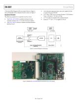
Circuit Note A functional block diagram of the test setup is shown in Figure 4, and a photograph of the evaluation board is shown in Figure 5. Equipment Needed The following equipment is required to test the circuit: POWER SUPPLY Figure 4. Functional Diagram of Test Setup The EVAL-AD7625EDZ modified evaluation board (includes software and 7 V dc wall wart power supply) The EVAL-CED1Z converter evaluation and demonstration platform board A low distortion signal generator, such as the Agilent 81150A or Audio Precision SYS2702 A PC with a USB 2.0 port running Windows® XP, Windows Vista, or...
カタログの4ページ目を開く
Circuit Note LEARN MORE Data Sheets and Evaluation Boards CN-0307 Design Support Package: http://www.analog.com/CN0307-DesignSupport Ardizzoni, John, and Jonathan Pearson, High Speed Differential ADC Driver Design Considerations, Application Note AN-1026, Analog Devices, Inc. Ardizzoni, John. “A Practical Guide to High-Speed PrintedCircuit-Board Layout,” Analog Dialogue 39-09, September 2005. AN-742 Application Note, Frequency Domain Response of Switched Capacitor ADCs. Analog Devices. ADA4897-2 Data Sheet AD8031 Data Sheet AD8032 Data Sheet ADR434 Datasheet REVISION HISTORY AN-827...
カタログの5ページ目を開くAnalog Devices/アナログ・デバイセズのすべてのカタログと技術パンフレット
-
 HMC722LP3E
8 ページ
-
 HMC853 Data Sheet
10 ページ
-
 AN-1084
8 ページ
-
 AN-1091
2 ページ
-
 AN_737
8 ページ
-
 AN-0982
4 ページ
-
 ADF7024
24 ページ
-
 AD9915
48 ページ
-
 AD9914
48 ページ
-
 ADRF6612
59 ページ
-
 ADRF6820
48 ページ
-
 ADL5246
32 ページ
-
 ADA4961
22 ページ
-
 AN-1141
8 ページ
-
 AN-698
36 ページ
-
 Temperature Sensors
2 ページ
-
 Reference Circuits
8 ページ
-
 Precision ADCs
16 ページ