
カタログの抜粋
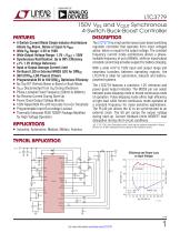
LTC3779 150V VIN and VOUT Synchronous 4-Switch Buck-Boost Controller Description 4-Switch Current Mode Single Inductor Architecture Allows VIN Above, Below or Equal to VOUT nn Wide V Range: 4.5V to 150V IN nn Wide Output Voltage Range: 1.2V ≤ V OUT ≤ 150V nn Synchronous Rectification: Up to 99% Efficiency nn ±1% 1.2V Voltage Reference nn Input or Output Average Current Limit nn On-Board LDO or External NMOS LDO for DRV CC nn 36V EXTV LDO Powers Drivers CC nn Programmable 6V to 10V DRV CC Optimizes Efficiency nn No Top FET Refresh Noise in Boost or Buck Mode nn V OUT Disconnected from VIN During Shutdown nn Phase-Lockable Fixed Frequency (50kHz to 600kHz) nn No Reverse Current During Start-Up nn Power Good Output Voltage Monitor nn 150V Rated RUN Pin with Accurate Turn-On Threshold nn Programmable Input Overvoltage Lockout nn Thermally Enhanced FE38 TSSOP Package Modified for High Voltage Operation nn The LTC®3779 is a high performance buck-boost switching regulator controller that operates from input voltages above, below or equal to the output voltage. The constant frequency current mode architecture allows a phaselockable frequency of up to 600kHz, while an input/output constant current loop provides support for battery charging. With a wide 4.5V to 150V input and output range and seamless transfers between operating regions, the LTC3779 is ideal for automotive, telecom and batterypowered systems. The LTC3779 features a precision 1.2V reference and power good output indicator. The MODE pin can select between pulse-skipping mode or forced continuous mode of operation. Pulse-skipping mode offers high efficiency at light load while forced continuous mode operates at a constant frequency for noise sensitive applications. The PLLIN pin allows the IC to be synchronized to an external clock. The SS pin ramps the output voltage during start-up. Current foldback limits MOSFET heat dissipation during short-circuit conditions. L, LT, LTC, LTM, Linear Technology and the Linear logo are registered trademarks of Analog Devices, Inc. All other trademarks are the property of their respective owners. Industrial, Automotive, Medical, Military, Avionics Efficiency and Power Loss vs Input Voltage SENSEN SGND POWER LOSS
カタログの1ページ目を開く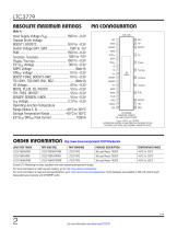
FE PACKAGE VARIATION: FE38(31) 38-LEAD PLASTIC TSSOP Tjmax = 150°C, 0ja = 28°C/W EXPOSED PAD (PIN 39) IS PGND, MUST BE SOLDERED TO PCB FOR RATED ELECTRICAL AND THERMAL CHARACTERISTICS LEAD FREE FINISH Consult LTC Marketing for parts specified with wider operating temperature ranges. For more information on lead free part marking, go to: http://www.linearcom/leadfree/ For more information on tape and reel specifications, go to: http://www.linear.com/tapeandreel/. Some packages are available in 500 unit reels through designated sales channels with #TRMPBF suffix.
カタログの2ページ目を開く
LTC3779 Electrical Characteristics Note 1: Stresses beyond those listed under Absolute Maximum Ratings may cause permanent damage to the device. Exposure to any Absolute Maximum Rating condition for extended periods may affect device reliability and lifetime. Note 2: The LTC3779 is tested under pulsed load conditions such that TJ ≈ TA. The LTC3779E is guaranteed to meet performance specifications from 0°C to 85°C junction temperature. Specifications over the –40°C to 125°C operating junction temperature range are assured by design, characterization and correlation with statistical process...
カタログの5ページ目を開く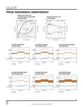
LTC3779 Typical Performance Characteristics Efficiency and Power Loss vs Load Current and Input Voltage Continuous Mode 96 POWER LOSS Efficiency and Power Loss vs Input Voltage Load Step Boost Region Continuous Mode Load Step Boost Region Pulse-Skipping Mode Load Step Buck-Boost Region Continuous Mode Load Step Buck-Boost Region Pulse-Skipping Mode Load Step Buck Region Continuous Mode Load Step Buck Region Pulse-Skipping Mode
カタログの6ページ目を開く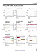
LTC3779 Typical Performance Characteristics Forced Continuous Mode Boost Region Forced Continuous Mode Buck-Boost Region Pulse-Skipping Mode Boost Region Forced Continuous Mode Buck Region Pulse-Skipping Mode Buck-Boost Region Pulse-Skipping Mode Buck Region Start-Up from RUN Forced Continuous Mode Pre-Biased Output Start-Up Forced Continuous Mode Boost Region Start-Up Forced Continuous Mode Buck-Boost Region 2.5ms/DIV VIN = 24V VOUT = 48V VOUT PRE-BIAS = 12V 200mA LOAD 5ms/DIV VIN = 24V VOUT = 48V 15Ω RESISTIVE LOAD 5ms/DIV VIN = 48V VOUT = 48V 15Ω RESISTIVE LOAD
カタログの7ページ目を開く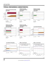
Start-Up Forced Continuous Mode Buck Region Shutdown from RUN Forced Continuous Mode Boost Region Shutdown from RUN Pulse-Skipping Mode Boost Region Vout = 48 V 15fi RESISTIVE LOAD Shutdown from RUN Forced Continuous Mode Buck-Boost Region Shutdown from RUN Forced Continuous Mode Buck Region Line Transient Rising Edge Line Transient Falling Edge DRVCC vs Load Current DRVCC vs Load Current - V/|N LDO (No NDRV FET), EXTVCC = 0V NDRV LDO (NDRV FET), EXTVCC = 0V EXTVCC = 8.5V (No NDRV FET)
カタログの8ページ目を開く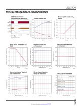
LTC3779 Typical Performance Characteristics VINOV Transient Forced Continuous Mode Buck Region Peak Current Threshold vs VITH (Boost) Current Foldback Limit 10ms/DIV VIN = 120V VOUT = 48V 50Ω RESISTIVE LOAD CURRENT LIMIT (SENSEP – SENSEN) (mV) CURRENT LIMIT (SENSEP – SENSEN) (mV) Valley Current Threshold vs VITH (Buck) V5 Low Dropout Regulation Voltage vs Temperature 12 DRVSET = V5 DRVSET = 3/4 • V5 DRVSET = 1/2 • V5 DRVSET = 1/4 • V5 Undervoltage Lockout Threshold (V5) vs Temperature CURRENT LIMIT (SENSEP – SENSEN) (mV) CURRENT LIMIT (SENSEP – SENSEN) (mV) Regulated Feedback Voltage vs...
カタログの9ページ目を開く
pin FuncTions BG1/BG2 (Pins 1 and 19): Bottom Gate Driver Outputs. This pin drives the gate(s) of the bottom N-Channel MOSFET between PGND to DRVcc. VINOV (Pin 2): Connect to the input supply through a resistor divider to set the over-voltage lockout level. A voltage on this pin above 1.28V disables all switching, and the top GATE pins are held low, the bottom GATE pins are held high, and VOUT is disconnected from VIN. DRVCC and V5 regulation is maintained during an over-voltage event. Normal operation resumes when the voltage on this pin decreases below 1.23V. Exceeding the VINOV...
カタログの11ページ目を開くADI/リニアテクノロジーのすべてのカタログと技術パンフレット
-
 LTC2068
30 ページ
-
 LTC6373
34 ページ
-
 ADL9006
16 ページ
-
 ADL8104
23 ページ
-
 AD4115
52 ページ
-
 ADUM7702
22 ページ
-
 AD7383
33 ページ
-
 AD7384
33 ページ
-
 AD4114
49 ページ
-
 ADUM7704
22 ページ
-
 AD7134
86 ページ
-
 LTspice IV
53 ページ
-
 New Products Catalog
43 ページ
-
 RF/IF Amplifiers
9 ページ
-
 SAR ADC Drivers
2 ページ
-
 SmartMesh Brochure
8 ページ
-
 INDUSTRIAL SIGNAL CHAIN
24 ページ
-
 Wireless & RF Solution
36 ページ
-
 LT6656 - 1
18 ページ


カタログアーカイブ
-
 New Products Catalog
39 ページ


