
カタログの抜粋
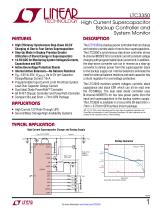
LTC3350 High Current Supercapacitor Backup Controller and System Monitor Description Features High Efficiency Synchronous Step-Down CC/CV Charging of One to Four Series Supercapacitors n Step-Up Mode in Backup Provides Greater Utilization of Stored Energy in Supercapacitors n 14-Bit ADC for Monitoring System Voltages/Currents, Capacitance and ESR n Active Overvoltage Protection Shunts n Internal Active Balancers—No Balance Resistors n V : 4.5V to 35V, V IN CAP(n): Up to 5V per Capacitor, Charge/Backup Current: 10+A n Programmable Input Current Limit Prioritizes System Load Over Capacitor Charge Current n Dual Ideal Diode PowerPath™ Controller n All N-FET Charger Controller and PowerPath Controller n Compact 38-Lead 5mm × 7mm QFN Package n Applications High Current 12V Ride-Through UPS Servers/Mass Storage/High Availability Systems The LTC®3350 is a backup power controller that can charge and monitor a series stack of one to four supercapacitors. The LTC3350’s synchronous step-down controller drives N‑channel MOSFETs for constant current/constant voltage charging with programmable input current limit. In addition, the step-down converter can run in reverse as a step-up converter to deliver power from the supercapacitor stack to the backup supply rail. Internal balancers eliminate the need for external balance resistors and each capacitor has a shunt regulator for overvoltage protection. The LTC3350 monitors system voltages, currents, stack capacitance and stack ESR which can all be read over the I2C/SMBus. The dual ideal diode controller uses N-channel MOSFETs for low loss power paths from the input and supercapacitors to the backup system supply. The LTC3350 is available in a low profile 38-lead 5mm × 7mm × 0.75mm QFN surface mount package. L, LT, LTC, LTM, Linear Technology and the Linear logo are registered trademarks and PowerPath are trademarks of Linear Technology Corporation. All other trademarks are the property of their respective owners. Patents pending. Typical Application High Current Supercapacitor Charger and Backup Supply ICHG (STEP-DOWN) IBACKUP VOUT Backup Operation INFET VOUTSP VOUTSN PFI OUTFB OUTFET TGATE VCAP < VOUT (STEP-UP) VCAP > VOUT (DIRECT CONNECT) ICAP VCAP CAP4 CAP3 CAP2 CAP1 CAPRTN CAPFB 400ms/DIV BACK PAGE APPLICATION CIRCUIT
カタログの1ページ目を開く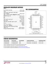
LTC3350 Absolute Maximum Ratings Pin Configuration VOUTM5 UHF PACKAGE 38-LEAD (5mm × 7mm) PLASTIC QFN TJMAX = 125°C, θJA = 34°C/W EXPOSED PAD (PIN 39) IS PGND, MUST BE SOLDERED TO PCB Order Information LEAD FREE FINISH PART MARKING PACKAGE DESCRIPTION TEMPERATURE RANGE Consult LTC Marketing for parts specified with wider operating temperature ranges. Consult LTC Marketing for information on nonstandard lead based finish parts. For more information on lead free part marking, go to: http://www.linear.com/leadfree/ For more information on tape and reel specifications, go to:...
カタログの3ページ目を開く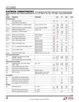
The l denotes the specifications which apply over the specified operating junction temperature range, otherwise specifications are at TA = 25°C (Note 2). VIN = VOUT = 12V, VDRVCC = VINTVCC unless otherwise noted. SYMBOL Input Supply Voltage Input Quiescent Current (Note 4) Maximum Regulated VCAP Feedback Voltage 4 VCAPDAC Full Scale (1111b) Minimum Regulated VCAP Feedback Voltage VCAPDAC Zero Scale (0000b) CAPFB Input Leakage Current Regulated VOUT Feedback Voltage OUTFET Turn-Off Threshold Falling Threshold OUTFB Input Leakage Current VOUT Voltage in Step-Up Mode INTVCC Undervoltage...
カタログの4ページ目を開く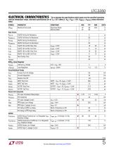
The l denotes the specifications which apply over the specified operating junction temperature range, otherwise specifications are at TA = 25°C (Note 2). VIN = VOUT = 12V, VDRVCC = VINTVCC unless otherwise noted. SYMBOL Maximum Duty Cycle Step-Down Mode Step-Up Mode Gate Drivers RUP-TG TGATE Pull-Up On-Resistance TGATE Pull-Down On-Resistance BGATE Pull-Up On-Resistance BGATE Pull-Down On-Resistance TGATE 10% to 90% Rise Time TGATE 10% to 90% Fall Time BGATE 10% to 90% Rise Time BGATE 10% to 90% Fall Time Non-Overlap Time INTVCC Linear Regulator VINTVCC Load Regulation PowerPath/Ideal...
カタログの5ページ目を開く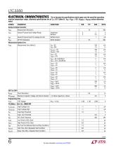
The l denotes the specifications which apply over the specified operating junction temperature range, otherwise specifications are at TA = 25°C (Note 2). VIN = VOUT = 12V, VDRVCC = VINTVCC unless otherwise noted. SYMBOL Analog-to-Digital Converter VRES Measurement Resolution General Purpose Input Voltage Range Unbuffered Buffered General Purpose Input Pin Leakage Current Buffered Input Buffer Disabled Measurement System Error VIN = 0V VIN = 30V Measurement Error (Note 5) VGPI = 0V, Unbuffered VGPI = 3.5V, Unbuffered Shunt Resistance Maximum Capacitor Voltage with Shunts Enabled 2 or More...
カタログの6ページ目を開く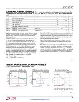
The l denotes the specifications which apply over the specified operating junction temperature range, otherwise specifications are at TA = 25°C (Note 2). VIN = VOUT = 12V, VDRVCC = VINTVCC unless otherwise noted. SYMBOL Stop Condition Set-Up Time Output Data Hold Time Input Data Hold Time Data Set-Up Time Input Spike Suppression Pulse Width SMBALERT Output Low Voltage SMBALERT High-Z Leakage Current Note 1: Stresses beyond those listed under Absolute Maximum Ratings may cause permanent damage to the device. Exposure to any Absolute Maximum Rating condition for extended periods may affect...
カタログの7ページ目を開く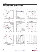
LTC3350 Typical Performance Characteristics TA = 25°C, Application Circuit 4 unless otherwise noted. IIN and ICHARGE vs VIN Load Regulation in Boost Mode 5.000 VCAP = 2V VCAP = 3V VCAP = 4V Efficiency in Boost Mode Charger Efficiency vs VCAP VCAP = 2V VCAP = 3V VCAP = 4V
カタログの8ページ目を開く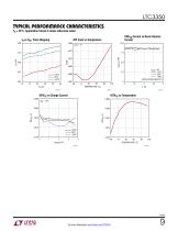
LTC3350 Typical Performance Characteristics TA = 25°C, Application Circuit 4 unless otherwise noted. INTVCC vs Charge Current DRVCC Current vs Boost Inductor Current
カタログの9ページ目を開く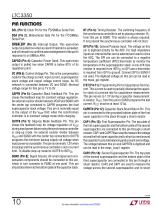
LTC3350 Pin Functions SCL (Pin 1): Clock Pin for the I2C/SMBus Serial Port. SDA (Pin 2): Bidirectional Data Pin for the I2C/SMBus Serial Port. SMBALERT (Pin 3): Interrupt Output. This open-drain output is pulled low when an alarm threshold is exceeded, and will remain low until the acknowledgement of the part’s response to an SMBus ARA. CAPGD (Pin 4): Capacitor Power Good. This open-drain output is pulled low when CAPFB is below 92% of its regulation point. VC (PIN 5): Control Voltage Pin. This is the compensation node for the charge current, input current, supercapacitor stack voltage and...
カタログの10ページ目を開くADI/リニアテクノロジーのすべてのカタログと技術パンフレット
-
 LTC2068
30 ページ
-
 LTC6373
34 ページ
-
 ADL9006
16 ページ
-
 ADL8104
23 ページ
-
 AD4115
52 ページ
-
 ADUM7702
22 ページ
-
 AD7383
33 ページ
-
 AD7384
33 ページ
-
 AD4114
49 ページ
-
 ADUM7704
22 ページ
-
 AD7134
86 ページ
-
 LTspice IV
53 ページ
-
 New Products Catalog
43 ページ
-
 RF/IF Amplifiers
9 ページ
-
 SAR ADC Drivers
2 ページ
-
 SmartMesh Brochure
8 ページ
-
 INDUSTRIAL SIGNAL CHAIN
24 ページ
-
 Wireless & RF Solution
36 ページ
-
 LT6656 - 1
18 ページ


カタログアーカイブ
-
 New Products Catalog
39 ページ


