
カタログの抜粋

■ Wide Input Voltage Range: 1.8V to 20V ■ Adjustable Output: 1.220V Reference Voltage ■ Shutdown Quiescent Current: <1uA ■ Stable with 10uF/3.3uF Minimum Output Capacitor ■ Stable with Ceramic, Tantalum or Aluminum Electrolytic Capacitors ■ Precision Threshold for Shutdown Logic or UVLO Function ■ PWRGD Flag for each Output ■ Reverse Battery and Reverse Output-to-input ■ Current Limit with Foldback and Thermal Shutdown ■ Thermally Enhanced 20-Lead TSSOP and ■ General Purpose Linear Regulator ■ Microprocessor Core/Logic Supplies ■ Post Regulator for Switching Supplies ■ Tracking/Sequencing Power Supplies XT, LT, LTC, LTM, Linear Technology and the Linear logo are registered trademarks and ThinSOT is a trademark of Linear Technology Corporation. All other trademarks are the property of their respective owners. icropower Linear Regulator The LT®3030isadual, micropower, lownoise, lowdropout linear regulator. The device operates with either common or independent input supplies for each channel, over a 1.8Vto 20V input voltage range. Output 1/Output 2 supply 750mA/250mA respectively with a typical dropout voltage of 300mV. With an external 10nF bypass capacitor, output noise is only 20UVRMS over a 10Hz to 100kHz bandwidth. Designed for use in battery-powered systems, the low 120uA/75uA quiescent current makes it an ideal choice. In shutdown, quiescent current drops to less than 1uA. Shutdown control is independent for each channel and its precision logic threshold allows for voltage lockout functionality. The LT3030 includes a PWRGD flag for each channel to indicate output regulation. The LT3030 optimizes stability and transient response with low ESR ceramic output capacitors, requiring a minimum Internal circuitry provides reverse-battery protection, reverse-current protection, current limiting with foldback and thermal shutdown with hysteresis. The adjustable output voltage device has a 1.220V reference voltage. The LT3030 is offered in the thermally enhanced 20-lead TVPicni nppucnTion Dropout Voltage vs Load Current ^^^J TECHNOLOGY
カタログの1ページ目を開く
ABSOLUTE mnximum Rnnnos Operating Junction Temperature (Notes 2,12) Storage Temperature Range Lead Temperature (Soldering, 10 sec) EXPOSED PAD (PIN 29) IS GND, MUST BE SOLDERED TO PCB EXPOSED PAD (PIN 21) IS GND, MUST BE SOLDERED TO PCB ORD€R inFORfTMTIOn Consult LTC Marketing for parts specified with wider operating temperature ranges. *The temperature grade is identified by a label on the shipping container. For more information on lead free part marking, go to: http://www.linear.com/leadfree/ For more information on tape and reel specifications, go to: http://www.linear.com/tapeandreel/...
カタログの2ページ目を開く
€l€CTRICni CHniMCTCRISTICS The • denotes the specifications which apply over the full operating temperature range, otherwise specifications are at TA = 25°C (Note 2). ^^^J TECHNOLOGY
カタログの3ページ目を開く
The • denotes the specifications which apply over the full operating temperature range, otherwise specifications are at TA = 25°C (Note 2). Note 1: Stresses beyond those listed under Absolute Maximum Ratings may cause permanent damage to the device. Exposure to any Absolute Maximum Rating condition for extended periods may affect device Note 2: The LT3030 is tested and specified under pulse load conditions such that Tj« TA. The LT3030E is 100% tested at TA = 25°C and performance is guaranteed from 0°C to 125°C. Performance of the LT3030E over the full -40°C to 125°C operating junction...
カタログの4ページ目を開く
TVPICRL p€RFORmnnc€ CHnnncTCMSTics Tj = 25°C, unless otherwise noted. 0UT1 Typical Dropout Voltage 0UT2 Typical Dropout Voltage Quiescent Current Quiescent Current TECHNOLOGY For more information www.linear.com/3030
カタログの5ページ目を開く
TVPICRL p€RFORmnnc€ CHnnncTCMSTics Tj = 25°C, unless otherwise noted. Quiescent Current in Shutdown 0UT1 GND Pin Current 0UT2 GND Pin Current 0UT2 GND Pin Current OUTPUT CURRENT (mA) INPUT VOLTAGE (V) INPUT VOLTAGE (V) ^^^J TECHNOLOGY
カタログの6ページ目を開く
TVPICRL p€RFORmnnc€ CHnnncTCMSTics Tj = 25°C, unless otherwise noted. Reverse Current
カタログの7ページ目を開く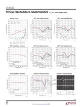
TVPICRL p€RFORmnnc€ CHnnncTCMSTics Tj = 25°C, unless otherwise noted. Reverse Current 0UT1 Input Ripple Rejection 0UT1 Input Ripple Rejection lADJ = FLOWS INTO ADJ PIN TO GND PIN 0UT1 Input Ripple Rejection 0UT2 Input Ripple Rejection 0UT2 Input Ripple Rejection
カタログの8ページ目を開く
LT3030 Typical Performance Characteristics ∆IL = 1mA TO FULL LOAD 4 6 4 ∆VIN = 2V TO 20V 2 0 –2 –4 2 1 0 –1 –2 –6 –3 –8 –4 –10 –75 –50 –25 0 25 50 75 100 125 150 175 TEMPERATURE (°C) –5 –75 –50 –25 0 25 50 75 100 125 150 175 TEMPERATURE (°C) 3030 G37 VOUT = 5V CBYP = 100pF VOUT = VADJ 0.1 CBYP = 0.01µF 0.1 140 1 10 FREQUENCY (Hz) 120 OUTPUT2 OUTPUT1 100 80 60 VOUT = 1.220V 40 OUTPUT1 100 0 10 0.1 1 10 FREQUENCY (kHz) 100 100 3030 G39 160 140 TJ = 25°C COUT = 10µF 120 VOUT1 = 5V CBYP1 = 0 100 80 VOUT1 = VADJ1 CBYP1 = 0 60 40 VOUT1 = VADJ1 1000 10000 VOUT1 = 5V 0 0.01 0.1 CBYP1 = 10nF 1 10...
カタログの9ページ目を開く
Tj = 25°C, unless otherwise noted.
カタログの10ページ目を開く
LT3030 Pin Functions (QFN/TSSOP) OUT1, OUT2 (Pins 1, 2, 7, 8/Pins 3, 4, 7, 8): Output. The OUT1/OUT2 pins supply power to the loads. A minimum 10μF/3.3μF output capacitor prevents oscillations on OUT1/OUT2. Applications with large output load transients require larger values of output capacitance to limit peak voltage transients. See the Applications Information section for more on output capacitance and on reverse output characteristics. GND (Pins 3, 4, 5, 6, 11, 12, 13, 18, 19, 24, 25, 26, Exposed Pad Pin 29/Pins 5, 6, 15, 16, Exposed Pad Pin 21): Ground. The exposed pad (backside) of the...
カタログの11ページ目を開く
nppucnuons inFOftmnnon with independent inputs, micropower quiescent current and shutdown. The device supplies up to 750mA/250mA from the outputs of channel 1 /channel 2 at atypical d ropout voltage of 300mV. The two regulators share common GND pins and are thermally coupled. However, the two inputs and outputs of the LT3030 operate independently. Each channel can be shut down independently, but a thermal shutdown fault on either channel shuts off the output on both channels. Theaddition of a 10nF reference bypass ca- pacitor lowers output voltage noiseto 20UVRMS overa 10Hz to 100kHz...
カタログの12ページ目を開くADI/リニアテクノロジーのすべてのカタログと技術パンフレット
-
 LTC2068
30 ページ
-
 LTC6373
34 ページ
-
 ADL9006
16 ページ
-
 ADL8104
23 ページ
-
 AD4115
52 ページ
-
 ADUM7702
22 ページ
-
 AD7383
33 ページ
-
 AD7384
33 ページ
-
 AD4114
49 ページ
-
 ADUM7704
22 ページ
-
 AD7134
86 ページ
-
 LTspice IV
53 ページ
-
 New Products Catalog
43 ページ
-
 RF/IF Amplifiers
9 ページ
-
 SAR ADC Drivers
2 ページ
-
 SmartMesh Brochure
8 ページ
-
 INDUSTRIAL SIGNAL CHAIN
24 ページ
-
 Wireless & RF Solution
36 ページ
-
 LT6656 - 1
18 ページ


カタログアーカイブ
-
 New Products Catalog
39 ページ


