- Catalogs
- TDK Electronics Europe
- Flip Chip Bonder
Flip Chip Bonder
1 /1Page

Flip Chip Bonder
1 /1Page
Catalog excerpts
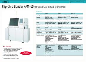
Specifications AFM-15AFM-22MDM-20Bonding Process Gold-to-gold interconnectionHeat compressionGlue dispensing(ultra sonic)(NCP, ACP, NCF, ACF, C4 and etc) Products TCXO, SAW, OPTO,Module, OPTO and etcAll of left productsHigh Frequency and etc IC MAX: 5.0W x 5.0D x 1.0T mmMAX: 30W x 30D x 0.635T mmΖMIN: 0.3W x 0.3D x 0.1T mmMIN: 3W x 3D x 0.25T mm Board MAX: 180W x 120D x 3.2T mmMAX: 180W x 120D x 1.6T mmMAX: 200W x 150D x 2.0T mmMIN: 50W x 50D x 0.3T mmMIN: 50W x 50D x 0.4T mmMIN: 30W x 30D x 0.3T mm Cycle Time 0.8sec/IC5.0sec/IC֖(excluding bonding process time)(excluding bonding process time) Accuracy 8 ѵ m/3 σ 3 ѵ m/3 σ 10 ѵ m(nozzle positioning accuracy) MAX Load 20N (special 100N) 372.4N IC Supply 5/6 inch wafer (8 inch option)2inch tray and etc֖ θ axis correctionHot blow Production management data Machine size Option and 1,200W x 1,450D x 1,550H mm 750W x 910D x 1,760H mm 740W x 1,140D x 1,550H mm Magazine Loader/UnloaderMagazine Loader/UnloaderMagazine Loader/Unloader Machine weight Special Features 2,000kg 1,100kg 680 kg IonizerIonizerPost heater table Carrier handling3.4inch trayCarrier handlingHepa-filter6inch waferDispensing monitoring Plasma cleaning unitLow pressure capability (min: 10g)Sylinge temperature adjustment Load/US sampling Nozzle surface monitoring 8 inch wafer Map data High accuracy mode Standard Features Pre/Mounting heater tableMounting heater tableVarious dispensing featuresNozzle auto cleaning & monitoringHepa-filterNozzle auto cleaning US checkingParallelism verificationPre/Dispense heater table IC height measurementBonding position verificationHeight detection Bump detectionTemperature calibrationProduction management data Wafer expandProduction management data Wafer > ? For High Precision Cost-Sensitive Applications All in one process for mounting and bonding? High Speed and Accuracy Mounting m? Small Footprint: Speed: 0.8 sec/IC Chip Component Accuracy: +/- 8 1.7 Square Meters? Easy Operation with Color Touch Screen? Inspection of Known Good Die from wafer? Capable to handle FR4, Ceramic or Silicon No CleanNo Lead Process >
Open the catalog to page 1All TDK Electronics Europe catalogs and technical brochures
 PTC Thermistors
28 Pages
 SATA SSD
3 Pages
 CF CARD
3 Pages
 Humidity Sensor CHS Series
11 Pages
 Color Video Camera
2 Pages
 EFE300M / EFE400M 300/400
4 Pages
 Piezoelectric Receiver RU
2 Pages
 Chip Beads STD
29 Pages
 Piezoelectric Type LTS, TSP
9 Pages
 Feed-back Type EFS
4 Pages
 SMD NTCG
14 Pages
 E Series
45 Pages
 Multilayer/Q-up MLG0402Q
5 Pages
 Pin Terminal Type PFC
14 Pages
 Ferrite Magnets FB
27 Pages
 NTC Thermistors SMD
14 Pages
 Wound Type SMD Inductors (Coils)
12 Pages
 Multilayer Chip Beads
27 Pages
 TDK MLCC CATALOG b11
72 Pages


![[BHF/BHP] Series for Barcode Printers, and Label Printers](https://img.directindustry.com/pdf/repository_di/34778/bhf-bhp-series-barcode-printers-label-printers-374455_1mg.jpg)


Archived catalogs
 EMC and RF testing
4 Pages
 RF Integrated Test Systems
12 Pages
 Microwave Absorbers
16 Pages
 Power supplies catalog
24 Pages
 Planar Cores
8 Pages
 Toroidal Cores
2 Pages
 Ferrite Electrodes
4 Pages


- Temperature probe
- Transformer
- Test cabinet
- Dry transformer
- Surge protector
- Resistance temperature sensor
- Level probe
- Liquid level sensor
- TDK capacitor
- Position transducer
- Current transformer
- Waterproof temperature sensor
- TDK electronic filter
- Power transformer
- Current sensor
- Industrial transformer
- Isolation transformer
- Passive electronic filter
- No-contact position sensor
- Solid-state drive