- Catalogs
- STMicroelectronics
- Rad-hard 4.5 A dual low-side MOSFET driver
Rad-hard 4.5 A dual low-side MOSFET driver
1 /31Pages

Rad-hard 4.5 A dual low-side MOSFET driver
1 /31Pages
Catalog excerpts

RHFPM4424 Rad-hard 4.5 A dual low-side MOSFET driver Datasheet - production data Applications • Switch mode power supply • DC-DC converters • Motor controllers • Line drivers Description Features • Wide operating voltage range: 4.5 V to 18 V • Parallel driving capability up to 9 A • Non-inverting configuration • Input 5 V logic level compatibility • 110 ns typical propagation delay • Matched propagation delays between the two channels (5 ns max.) • 20 mV maximum low level output voltage • 30 ns rise and fall times • +/-5 V common mode bouncing between signal and power grounds • TID: – 300 krad HDR – 100 krad LDR The RHFPM4424 is a flexible, high-frequency dual low-side driver specifically designed to work with high capacitive MOSFETs and IGBTs in a high radiation environment such as the aerospace. The RHFPM4424 outputs can sink and source 4.5 A of peak current independently. By putting in parallel the two PWM outputs, a higher driving current (up to 9 A peak) can be obtained. The RHFPM4424 works with CMOS/TTL compatible PWM signal so it can be driven by an external PWM controller, for instance the ST1843 or the ST1845. The hermetic FLAT-16 version has an industry standard pinout and it can dissipate up to 1.5 W (750 mW per channel), while FLAT-10 version optimizes the PCB real estate. Both of packages are hermetic, making the device wellsuited for any kind of harsh environment. • QML-V qualification planned • Hermetic package Order codes Engineering model Engineering model Temperature range Quality level EPPL Package 1. Contact ST sales office for information about the die specific conditions and for other quality levels. 2. Under development. December 2014 This is information on a product in full production.
Open the catalog to page 1
Typical application diagram . . . . . . . . . . . . . . . . . . . . . . . . . . . . . . . . . . . 7 Absolute maximum ratings . . . . . . . . . . . . . . . . . . . . . . . . . . . . . . . . . . . 8 Total ionizing dose (MIL-STD-883 test method 1019) . . . . . . . . . . . . . . . .11 TID and HI results . . . . . . . . . . . . . . . . . . . . . . . . . . . . . . . . . . . . . . . . . . .11 Device description and operation . . . . . . . . . . . . . . . . . . . . . . . . . . . . . 12 7.1 7.2 Parallel output operation . . . . . . . . . . . . . . . . . . . . . . . . . . . . . . . . . . . . . 13 Gate...
Open the catalog to page 2
Date code . . . . . . . . . . . . . . . . . . . . . . . . . . . . . . . . . . . . . . . . . . . . . . . . . 28 Documentation . . . . . . . . . . . . . . . . . . . . . . . . . . . . . . . . . . . . . . . . . . . . . 29
Open the catalog to page 3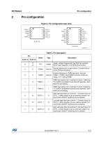
Pin configuration Figure 2. Pin configuration (top view) Table 2. Pin description Pin Name Supply voltage. Bypass with low ESR (for example MLCC type) capacitor to the PCB ground plane. Ground reference for output drivers. Connect this pin to the PCB ground plane. Ground reference for PWM input pins. Input pin (PWM_1, PWM_2 and SGND) common mode can range +/-5 V versus PGND. PWM input signal (non-inverting) for driver 1 featuring TTL/CMOS compatible threshold and hysteresis. Don't leave the pin floating. PWM input signal (non-inverting) for driver 2 featuring TTL/CMOS compatible threshold and...
Open the catalog to page 5
RHFPM4424 Table 2. Pin description (continued) Pin Name Low-side open drain pin of driver 2. Connect this pin to OUTH_2 either directly or by an external resistor if an asymmetric ON/OFF switching time is desired. Not connected pin. Leave it floating or connect it to any potential.
Open the catalog to page 6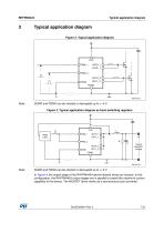
Typical application diagram Typical application diagram Figure 3. Typical application diagram SGND and PGND can be shorted or decoupled up to +/-5 V. Figure 4. Typical application diagram as buck switching regulator SGND and PGND can be shorted or decoupled up to +/-5 V. In Figure 4, the output stage of the RHFPM4424 device directly drives an inductor; in this configuration, the RHFPM4424 output stages are in parallel to exploit the maximum current capability of the device. The MOSFET driver works as a synchronous buck converter.
Open the catalog to page 7
Absolute maximum ratings Absolute maximum ratings Table 3. Thermal data Value Symbol Max. thermal resistance, junction-to-case Maximum power dissipation @ Tamb = 70 °C Table 4. Absolute maximum ratings Symbol Supply voltage Power ground Signal ground Driver output DC output current (for each driver) Storage temperature Maximum operating junction temperature Lead temperature (soldering, 10 seconds)(1) ESD capability, human body model ESD capability, machine model 1. The distance is 1.5 mm far from the device body and the same lead is resoldered after 3 minutes.
Open the catalog to page 8
Electrical characteristics Electrical characteristics VCC = 4.5 V to 18 V and TJ = -55 to 125 °C, unless otherwise specified. Table 5. Electrical characteristics Test conditions Undervoltage lockout threshold for turn-on Supply current and power-on Undervoltage lockout hysteresis Input stage Input at high level – VIH Rising threshold Falling threshold PWMx = SGND PWM_x input pin current dVPWM/dt PWM_x input pin transient(1) Output stage Source resistance VCC = 10 V Inputs at high level IOUT = 100 mA Tj = 25 °C Sink resistance VCC = 10 V Inputs at low level IOUT = 100 mA Tj = 25 °C VCC = 10 V...
Open the catalog to page 9
Electrical characteristics RHFPM4424 Table 5. Electrical characteristics (continued) Test conditions Sink peak current VCC = 10 V Inputs at low level COUT to GND = 10 nF High level output voltage, VCC-VOUT Inputs at high level OUTH_1 ≡ OUTL_1 OUTH_2 ≡ OUTL_2 IOUT = 1 mA Low level output voltage, VOUT Inputs at low level OUTH_1 ≡ OUTL_1 OUTH_2 ≡ OUTL_2 IOUT = 1 mA Output rise time Output fall time Propagation delay Input- to-output delay time Matching between propagation delays(1) 1. Parameter guaranteed at design level, not tested in production.
Open the catalog to page 10
Total ionizing dose (MIL-STD-883 test method 1019) The products guaranteed in radiation within RHA QML-V system fully comply with the MILSTD-883 test method 1019 specification. The RHFPM4424 is being RHA QML-V qualified, tested and characterized in full compliance with the MIL-STD-883 specification, both below 10 mrad/s and between 50 and 300 rad/s. • • ELDRS characterization is performed in qualification only on both biased and unbiased parts, on a sample of ten units from two different wafer lots. Testing is performed in accordance with MIL-PRF-38535 and the test method 1019 of the MIL-STD-883...
Open the catalog to page 11All STMicroelectronics catalogs and technical brochures
 STGW30NC60KD
14 Pages
 STGB14NC60K STGD14NC60K
16 Pages
 HD1750FX
8 Pages
 TDA75610SLV
42 Pages
 TDA7391
13 Pages
 TDA7376B
15 Pages
 TDA7375V
15 Pages
 TDA2005
25 Pages
 L4989D, L4989MD
19 Pages
 L4938ED L4938EPD
20 Pages
 L4949ED-E L4949EP-E
19 Pages
 L4925
L492514 Pages
 FDA903U
80 Pages
 FDA803U
76 Pages
 FDA903D
82 Pages
 FDA803D
78 Pages
 BALF-SPI2-02D3
13 Pages
 LIS2DTW12
65 Pages
 VL53L0X
40 Pages
 LPS22HH
59 Pages
 Standard products offer overview
13 Pages
 M40SZ100W
20 Pages
 A1C15S12M3
17 Pages
 TSX923
32 Pages
 TS1851
24 Pages
 LMV321
17 Pages
 Serial real-time clock (RTC) ICs
16 Pages
 TDA2003LG
8 Pages
 HCF4541 Programmable Timer
10 Pages
 STA8058 GPS multi-chip module
14 Pages
 TDA7410ND Signal Processor
34 Pages
 TDA7410ND Signal Processor
34 Pages
 TSA1204 DUAL CHANNEL
31 Pages


Archived catalogs
 NEATSwitch
6 Pages
 Power MOSFETs for metering
2 Pages


- Single-pole switch
- Acceleration sensor
- Pressure probe
- Technology switch
- Signal amplifying integrated circuit
- Multipole switch
- Piezoelectric accelerometer
- Transceiver module
- Electronic filter
- Electromechanical switch
- Membrane pressure sensor
- Analog pressure sensor
- Rotary electric switch
- Triaxial acceleration sensor
- Power amplifying integrated circuit
- Distance sensor
- Diode
- STMicroelectronics transistor
- Low-pass electronic filter
- Absolute pressure sensor