Group: STMicroelectronics

Catalog excerpts
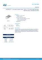
Features • ACEPACK™ 1 power module — DBC Cu AI2O3 Cu • Converter inverter brake topology - 1600 V, very low drop rectifiers for converter - Soft and fast recovery diode • Integrated NTC Applications • Inverters • Motor drives Description This power module is a converter-inverter brake (CIB) topology in an ACEPACK™ 1 package with NTC, integrating the advanced trench gate field-stop technology from STMicroelectronics. This new IGBT technology represents the best compromise between conduction and switching loss, to maximize the efficiency of any converter system up to 20 kHz. Product status DS11631 - Rev 6 - February 2018 For further information contact your local STMicroelectronics sales office.
Open the catalog to page 1
1 Electrical ratings1.1 Inverter stage Limiting values at Tj= 25 °C, unless otherwise specified. 1.1.1 IGBTs Table 1. Absolute maximum ratings of the IGBTs, inverter stage
Open the catalog to page 2
1.2 Brake stage Limiting values at Tj= 25 °C, unless otherwise specified. 1.2.1 IGBT Table 5. Absolute maximum ratings of the IGBT, brake stage
Open the catalog to page 4
1.3 Converter stage Limiting values at Tj= 25 °C, unless otherwise specified. Table 9. Absolute maximum ratings of the bridge rectifiers
Open the catalog to page 6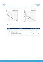
Figure 4. NTC resistance vs. temperature, zoom R (A) 800 700 600 500 400 300 85 90 95 100 105 110 Tc (°C) Table 12. ACEPACK™ 1 package
Open the catalog to page 7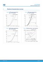
A1C15S12M3 Electrical characteristics (curves) Electrical characteristics (curves) Figure 5. IGBT output characteristics (VGE = 15 V, terminal) IC (A) Figure 6. IGBT output characteristics (TJ = 150 °C, terminal) IC (A) Figure 7. IGBT transfer characteristics (VCE = 15 V, terminal) IC (A) Figure 8. Switching energy vs. gate resistance E (mJ)
Open the catalog to page 8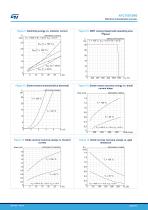
A1C15S12M3 Electrical characteristics (curves) Figure 9. Switching energy vs. collector current E (mJ) Figure 10. IGBT reverse biased safe operating area (RBSOA) IGBT021220161423FSOA Figure 11. Diode forward characteristics (terminal) IF (A) Figure 12. Diode reverse recovery energy vs. diode current slope Erec (mJ) Figure 13. Diode reverse recovery energy vs. forward current Erec (mJ) Figure 14. Diode reverse recovery energy vs. gate resistance Erec (mJ)
Open the catalog to page 9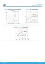
A1C15S12M3 Electrical characteristics (curves) Figure 15. Converter diode forward characteristics (terminal) IF (A) Figure 16. IGBT thermal impedance Zth(°C/W) Figure 17. Inverter diode thermal impedance Zth(°C/W)
Open the catalog to page 10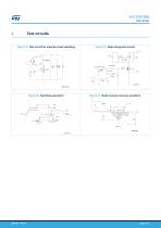
Test circuits Figure 18. Test circuit for inductive load switching Figure 19. Gate charge test circuit Figure 20. Switching waveform Figure 21. Diode reverse recovery waveform Td(off) Tr(Ion)
Open the catalog to page 11
Topology and pin description Figure 22. Electrical topology and pin description P Figure 23. Package top view with CIB pinout
Open the catalog to page 12
Package information In order to meet environmental requirements, ST offers these devices in different grades of ECOPACK® packages, depending on their level of environmental compliance. ECOPACK® specifications, grade definitions and product status are available at: www.st.com. ECOPACK® is an ST trademark.
Open the catalog to page 13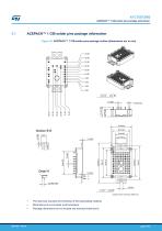
A1C15S12M3 ACEPACK™ 1 CIB solder pins package information ACEPACK™ 1 CIB solder pins package information Figure 24. ACEPACK™ 1 CIB solder pins package outline (dimensions are in mm) The lead size includes the thickness of the lead plating material. Dimensions do not include mold protrusion. Package dimensions do not include any eventu
Open the catalog to page 14
A1C15S12M3 Revision history Table 13. Document revision history
Open the catalog to page 15
Electrical characteristics (curves) . . . . . . . . . . . . . . . . . . . . . . . . . . . . . . . . . . . . . . . . . . . . . . . . . . 8 ACEPACK™ 1 CIB solder pins package information. . . . . . . . . . . . . . . . . . . . . . . . . . . . . . . . 13 Revision history . . . . . . . . . . . . . . . . . . . . . . . . . . . . . . . . . . . . . . . . . . . . . . . . . . . . . . . . . . . . . . . . . . . . . . .15 Contents . . . . . . . . . . . . . . . . . . . . . . . . . . . . . . . . . . . . . . . . . . . . . . . . . . . . . . . . . . . . . . . . . . . . . . . . . . . . . .16 Disclaimer . . . ....
Open the catalog to page 16
IMPORTANT NOTICE – PLEASE READ CAREFULLY STMicroelectronics NV and its subsidiaries (“ST”) reserve the right to make changes, corrections, enhancements, modifications, and improvements to ST products and/or to this document at any time without notice. Purchasers should obtain the latest relevant information on ST products before placing orders. ST products are sold pursuant to ST’s terms and conditions of sale in place at the time of order acknowledgement. Purchasers are solely responsible for the choice, selection, and use of ST products and ST assumes no liability for application...
Open the catalog to page 17All STMicroelectronics catalogs and technical brochures
-
 STGW30NC60KD
14 Pages
-
 STGB14NC60K STGD14NC60K
16 Pages
-
 HD1750FX
8 Pages
-
 TDA75610SLV
42 Pages
-
 TDA7391
13 Pages
-
 TDA7376B
15 Pages
-
 TDA7375V
15 Pages
-
 TDA2005
25 Pages
-
 L4989D, L4989MD
19 Pages
-
 L4938ED L4938EPD
20 Pages
-
 L4949ED-E L4949EP-E
19 Pages
-
 L4925
L492514 Pages
-
 FDA903U
80 Pages
-
 FDA803U
76 Pages
-
 FDA903D
82 Pages
-
 FDA803D
78 Pages
-
 BALF-SPI2-02D3
13 Pages
-
 LIS2DTW12
65 Pages
-
 VL53L0X
40 Pages
-
 LPS22HH
59 Pages
-
 Standard products offer overview
13 Pages
-
 M40SZ100W
20 Pages
-
 TSX923
32 Pages
-
 TS1851
24 Pages
-
 LMV321
17 Pages
-
 Serial real-time clock (RTC) ICs
16 Pages
-
 TDA2003LG
8 Pages
-
 HCF4541 Programmable Timer
10 Pages
-
 STA8058 GPS multi-chip module
14 Pages
-
 TDA7410ND Signal Processor
34 Pages
-
 TDA7410ND Signal Processor
34 Pages
-
 TSA1204 DUAL CHANNEL
31 Pages


Archived catalogs
-
 NEATSwitch
6 Pages
-
 Power MOSFETs for metering
2 Pages

