- Catalogs
- Sony Semiconductors
- CXD4017R
- Products
- Catalogs
- News & Trends
- Exhibitions
CXD4017R
1 /34Pages

CXD4017R
1 /34Pages
Catalog excerpts
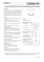
CXD4017R Reception Digital Signal Processor IC for Infrared Spatial Digital Audio Communication Description The CXD4017R is an IC that processes the received digital signals used for infrared spatial digital audio communication (based on the IEC61603-8-1 standard) in consumer products. This IC contains the analog-to-digital converter (ADC) for RF signal applications and a PLL circuit for audio applications. Features • Performs all the received digital signal processing on a single chip. • Supports the infrared spatial digital audio communication system formats for consumer uses. • Direct input of RF signals enabled by on-chip ADC. • External RAM and PLL circuit not required. 64 pin LQFP (Plastic) Structure Silicon gate CMOS IC Demodulator Block • Digital processing throughout enables the received RF signals in the infrared spatial digital audio communication system formats to be processed directly. • External analog circuit can be simplified by digital filter and on-chip ADC for RF signal applications. • Reproduction of subcarrier processed digitally. Error Corrector Block • Enables error correction for infrared spatial digital audio communication system formats. Output Interface Block • Digital-to-analog converter (DAC) for various audio applications can be connected directly. Controller Block • Simple pin setting mode • Serial interface provided by serial bus • Enables output of error correction state. Absolute Maximum Ratings • Supply voltage VDD1 –0.5 to +3.0 VDDE –0.5 to +3.0 • Input voltage VI –0.5 to VDDE + 0.5 (≤ 3.0V) • Output voltage VO –0.5 to VDDE + 0.5 (≤ 3.0V) • Storage temperature Tstg –55 to +125 °C Recommended Operating Conditions • Supply voltage VDDI 1.5 ± 0.1 2.5 ± 0.2 VDDE • A/D supply voltage VAD 2.5 ± 0.2 • PLL supply voltage VPLL 1.5 ± 0.1 • Operating temperature Topr –40 to +85 V V V V °C V V V V Input/Output Capacitance • Input capacitance CIN 16 (max.) pF • Output capacitance COUT 16 (max.) pF Note: Measurement conditions: Tj = 25°C, VDD = VI = 0V, f = 1MHz • Analog input capacitance 12 (typ.) pF CAD PLL Block • On-chip PLL circuit for reproducing the clock signals required by the infrared spatial digital audio communication system formats. Sony reserves the right to change products and specifications without prior notice. This information does not convey any license by any implication or otherwise under any patents or other right. Application circuits shown, if any, are typical examples illustrating the operation of the devices. Sony cannot assume responsibility for any problems arising out of the use of these circuits. –1– E03970B49-PS
Open the catalog to page 1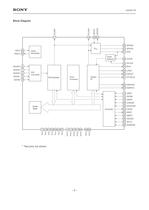
CXD4017R PLREF PLVAR APVCI APCPO Block Diagram 17 18 20 22 23 APAVD OSCI 40 OSCO 43 24 APAVS PLL Clock Generator 31 APX Clock Selector 28 VCOR 32 EXTCK ADVRH 6 ADAVS 7 ADAVD 8 ADVRL 9 54 BCK 59 LRCK A/D Converter 60 DAOUT Error Corrector Demodulator ADVIN 10 Output I/F 61 DTVALID 62 EMPFS0 63 EMPFS1 13 XRST 14 DIFM0 15 DIFM1 29 CHNUM 30 DIVCODE Buffer RAM Controller 33 CSOD 34 SRDT 35 SWDT 36 XSCEN 37 SCLK –2– VDDI VDDI ∗ Test pins not shown. VDDE VDDE VDDE VDDE VDDE VSS VSS VSS VSS 26 58 VSS 4 11 27 41 56 VSS 5 12 21 25 39 42 57 VSS 38 SCMODE
Open the catalog to page 2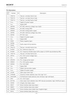
CXD4017R Pin Description Pin No. Symbol I/O Description 1 TEST12 I Test pin, normally fixed at low 2 TEST13 I Test pin, normally fixed at high 3 TEST14 I Test pin, normally fixed at high 4 VDDE — Digital I/O power supply 5 VSS — Digital GND 6 ADVRH I 7 ADAVS — RF ADC analog GND 8 ADAVD — RF ADC analog power supply 9 ADVRL I RF ADC reference voltage input (low) 10 ADVIN I RF ADC input 11 VDDE — Digital I/O power supply 12 VSS — Digital GND 13 XRST I 14 DIFM0 I 15 DIFM1 I 16 TEST15 I Test pin, normally fixed at low 17 PLREF O PLL reference output (fs) 18 PLVAR O PLL frequency-divided output (APX...
Open the catalog to page 4
CXD4017R Pin No. Symbol I/O 38 SCMODE I 39 VSS 40 OSCI I 41 VDDE — Digital I/O power supply 42 VSS — Digital GND 43 OSCO O Crystal oscillator circuit output (12.288MHz) 44 TEST0 I Test pin, normally fixed at low 45 TEST1 I Test pin, normally fixed at low 46 TEST2 I Test pin, normally fixed at low 47 TEST3 I Test pin, normally fixed at low 48 TEST4 I Test pin, normally fixed at low 49 TEST5 I Test pin, normally fixed at low 50 TEST6 I Test pin, normally fixed at low 51 TEST7 I Test pin, normally fixed at low 52 TEST8 O Test pin, normally open 53 TEST9 O Test pin, normally open 54 BCK O Bit clock...
Open the catalog to page 5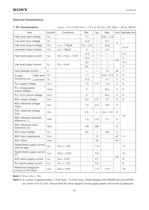
CXD4017R Electrical Characteristics 1. DC characteristics Item (VDDE = 2.5 ± 0.2V, VDDI = 1.5 ± 0.1V, VSS = 0V, Topr = –40 to +85°C) Symbol Conditions Min. Typ. Max. Unit Applicable pins High level input voltage VIH 1.7 — VDDE + 0.3 Low level input voltage VIL –0.3 — 0.7 High level output voltage VOH IOH = –100µA VDD – 0.2 — VDDE Low level output voltage VOL IOL = 100µA 0 — 0.2 High level output current IOH VOH = VDDE – 0.4V –4.0 — — –8.0 — — 4.0 — — 8.0 — — — — ±5 µA ∗1 Low level output current IOL Input leakage current VOL = 0.4V IL ∗1 V ∗ 2, 3, 4 ∗ 2, 3 mA ∗4 ∗ 2, 3 ∗4 High level VIH 1.7 VDDE...
Open the catalog to page 6
CXD4017R Applicable pins ∗ 1 XRST, DIFM0, DIFM1, VCOR, CHNUM, DIVCODE, EXTCK, SWDT, XSCEN, SCLK, SCMODE, TEST0 to TEST7, TEST11 to TEST16 ∗ 2 CSOD, LRCK, DAOUT, DTVALID, EMPFS0, EMPFS1, TEST8 ∗ 3 SRDT ∗ 4 PLREF, PLVAR, APX, BCK, TEST9, TEST10 ∗ 5 OSCI, OSCO ∗ 6 APAVD, APAVS ∗ 7 APCPO ∗ 8 APVCI ∗ 9 ADAVD, ADAVS ∗ 10 ADVRL, ADVRH ∗ 11 ADVIN ∗ 12 VDDI ∗ 13 VDDE –7–
Open the catalog to page 7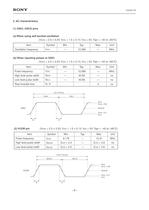
CXD4017R 2. AC characteristics (1) OSCI, OSCO pins (a) When using self-excited oscillation (VDDE = 2.5 ± 0.2V, VDDI = 1.5 ± 0.1V, VSS = 0V, Topr = –40 to +85°C) Item Symbol Min. Typ. Max. Unit — 12.288 — MHz fSYS Oscillation frequency (b) When inputting pulses to OSCI (VDDE = 2.5 ± 0.2V, VDDI = 1.5 ± 0.1V, VSS = 0V, Topr = –40 to +85°C) Item Symbol Min. Typ. Max. Unit Pulse frequency fSYS — 12.288 — MHz High level pulse width tWHX tWLX tR , tF — 40.69 — ns — 40.69 — ns 5 ns Low level pulse width Rise time/fall time tCX (1/fSYS) tWLX tWHX VIHX VIHX × 0.9 VDDE/2 OSCI VIHX × 0.1 VILX tF tR (2) VCOR...
Open the catalog to page 8All Sony Semiconductors catalogs and technical brochures
 IMX901-AMR
2 Pages
 IMX490
2 Pages
 IMX290NQV
2 Pages
 ISX016
2 Pages
 IMX390CQV
2 Pages
Archived catalogs
 SLD344YT
6 Pages
 SLD432S
5 Pages
 CXA3314ER
16 Pages
 CXB1818Q
17 Pages
 ICX205AK
24 Pages
 CXA2096N
17 Pages
 SLD433S4
5 Pages
 CXA4416GC
21 Pages
 CXA2984GC SP4T ANT SW
11 Pages
 SLD335YT
5 Pages
 CXM3807K
24 Pages
 CXM3648UR
11 Pages
 CXM3645ER
12 Pages
 CXM3642K
29 Pages
 CXM3641ER
22 Pages
 CXM3632ER
22 Pages
 CXM3630UR
15 Pages
 CXM3617ER
23 Pages
 CXM3614ER
14 Pages
 CXM3604UR
14 Pages
 CXM3599UR
15 Pages
 CXM3593UR
11 Pages
 SLD1332V
5 Pages
 CXM3592AUR
15 Pages
 CXM3583AUR
17 Pages
 CXM3582UR
17 Pages
 CXM3580UR
13 Pages
 CXM3580AUR
17 Pages
 CXM3572ER
14 Pages
 CXM3570ER
13 Pages
 CXM3569XR
13 Pages
 ICX418ALB
20 Pages
 CXD4728R
68 Pages
 ICX642BKA
23 Pages
 CXA3791EN
13 Pages
 SLD332F
6 Pages
 CXG1407XR
11 Pages
 IMX291LQR
2 Pages
 IMX252LLR/LQR
2 Pages
 IMX230
2 Pages
 IMX377CQT
5 Pages
 IMX249LLJ/LQJ
2 Pages
 IMX323LQN
2 Pages
 IMX258
2 Pages
 IMX302LQJ
2 Pages
 CXA3197R
30 Pages
 IMX222LQJ
2 Pages
 IMX324
2 Pages
 IMX367LLA
2 Pages
 IMX412-AACK
2 Pages
 IMX385LQR
2 Pages
 IMX294CJK
2 Pages
 IMX253LLR/LQR
2 Pages
 IMX273LLR/LQR
2 Pages
 IMX183CLK-J/CQJ-J
2 Pages
 IMX249LLJ/IMX249LQJ
2 Pages
 IMX250LLR/LQR,IMX252LLR/LQR
2 Pages
 B/W Video Camera CCD ICX422AL
17 Pages
 B/W Video Camera CCD ICX279AL*2
18 Pages
 Color Video Camera CCD ICX239AKE
18 Pages
 Color Video Camera CCD ICX418AKL
22 Pages


- Display module
- LCD display panel
- Color display panel
- LED display panel
- RGB display panel
- Compact display panel
- GNSS receiver
- Compact receiver
- Industrial receiver
- OLED display
- High-definition display module
- Laser diode
- Satellite receiver
- Sony CMOS image sensor
- Vision sensor
- Communication card
- Full HD display
- Codec
- Fiber laser diode
- Sony visible image sensor