- Catalogs
- Sony Semiconductors
- CXB1818Q
- Products
- Catalogs
- News & Trends
- Exhibitions
CXB1818Q
1 /17Pages

CXB1818Q
1 /17Pages
Catalog excerpts
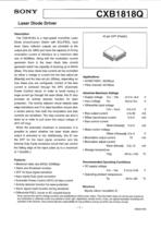
Laser Diode Driver The CXBT818Q is a high-speed monolithic Laser Diode Driver/Current Switch with ECL/PECL input level. Open collector outputs are provided at the output pins (Q, QBX) and have the capacity of driving modulation current of 50mAp-p at a maximum data rate of 622Mbps. Along with the modulation current generator there is the laser diode bias current generator which has capacity of sourcing up to 60mA (Bias). The laser diode bias current can be controlled by either a voltage or current into the bias adjust pin (BiasAdj) and the bias set pin (SBias), depending on how these pins are configured. Control of the bias current is achieved through the APC (Automatic Power Control) circuit. In order to avoid having a large current go through the laser diode, this IC also provides an Activity detector function for laser protection. The Activity detector circuit detects data edge transitions and if no data transition occurs after a certain period, then both the modulation and bias currents are shutdown. The bias currents are shut it down by in order to pull down the output voltage of When the automatic shutdown is conducted, it is possible to select whether the laser diode alarm output is activated or not. Additionally, this IC has the DFF for the input signal correction and the internal Duty Cycle correction circuit that can control the falling edge of the input pulse up to a maximum Absolute Maximum Ratings • Differential input voltage • Bias output current 0 to 80 mA • SBias input/output current 0 to 5 mA • Bias control current • Bbias control voltage ♦ Modulation output current 70 mA • Modulation adjust current • Storage temperature Recommended Operating Conditions • Operating ambient temperature • Maximum data rate (NRZ): 622Mbps • Alarm and Shutdown function • DFF for input signal correction • Input signal Duty cycle correction • Automatic Power Control (APC) for bias current • Activity detector function for laser protection • Alarm signal mask function during shutdown • Differential PECL inputs or AC coupled inputs Sony reserves the right to change products and specifications without prior notice. This information does not convey any license by any implication or otherwise under any patents or other right. Application circuits shown, if any, are typical examples illustrating the operation of the devices. Sony cannot assume responsibility for any problems arising out of the use of these circuits. Bipolar silicon monolithic IC
Open the catalog to page 1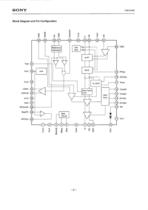
Block Diagram and Pin Configuration Duty Cycle
Open the catalog to page 2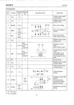
Equivalent circuit Positive power supply Negative power supply Bias current setting. Bias current setting or Bias current output. Open collector output. Negative power supply Modulation current Open collector output. Complementary current symmetrical output. Negative power supply Positive power supply Chip temperature
Open the catalog to page 3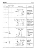
Equivalent circuit Modulation current driver compensation. Normally, connects CornpB pins. Capacitor connection (IN_ALM) operation. This pin sets the period activity detector. Activity detector circuit Activity detector selection control. High (open): (Through mode)
Open the catalog to page 4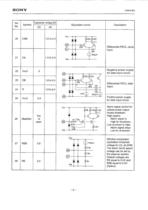
Equivalent circuit Differential PECL clock Negative power supply for data input circuit. Differential PECL data Positive power supply for data input circuit. Alarm signal control for optical power output forced shutdown. High (open): Alarm signal stays Window comparator top/bottom threshold The alarm (fault) assert
Open the catalog to page 5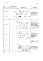
Equivalent circuit output current. (Shutdown input) When left open, High. Output duty cycle falling edge of the input High pulse. Variable delay limit of that is from a resistor value between compensated reference Positive power supply for alarm output circuit. laser monitor diode (Pseudo LVTTL output)
Open the catalog to page 6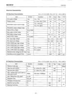
Electrical Characteristics
Open the catalog to page 8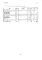
DC and AC Electrical Characteristics for OpAmp of APC Circuit
Open the catalog to page 9
Description of Each Function Block 1. Data Buffer, Clock Buffer Data Buffer and Clock Buffer are comprised of the data buffer, clock buffer, DFF, MUX and delay generator. ECL/PECL data is input to the data buffer at a maximum data rate of 622Mbps. The input data DFF selection pin {Pin 19 FFSel) can select whether the input data is used in through mode or the signal which is corrected by the clock signal in the DFF is used. When the FFSel is open, the data becomes through mode, when the FFsel is connected VEE.the data becomes DFF mode. And, this data is input to the delay circuit. The delay circuit...
Open the catalog to page 10
The laser diode alarm output state can be controlled by the alarm signal control pin (Pin 26 MaskSel) for the optical power output forced shutdown. When the automatic shutdown is conducted and MaskSel pin is left open, the laser diode alarm output goes High. The laser diode alarm output is kept Low (disable) by connecting 5. Shutdown and Input Alarm Circuits These circuits disable both the modulation current and the bias current under various conditions. The function block diagram for all of the shutdown mechanisms for the circuit is shown in Fig. 5. The Shutdown circuit has complementary TTL...
Open the catalog to page 11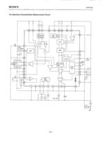
DC Electrical Characteristics Measurement Circuit
Open the catalog to page 12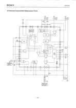
AC Electrical Characteristics Measurement Circuit
Open the catalog to page 13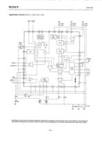
Application circuits shown are typical examples illustrating the operation of the devices. Sony cannot assume responsibility for any problems arising out of the use of these circuits or for any infringement of third party patent and other right due to same.
Open the catalog to page 14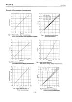
Example of Representative Characteristics Fig. 1. Pulse width vs. Rset characteristics when 1.6ns input data pulse (622Mbps) is applied IQset characteristics Fig. 3. Bias current (I BIAS) VS. Bias adjust current (IBset) characteristics Fig. 4. Bias current (IBIAS) vs. Bias adjust voltage (VBset) characteristics Fig. 6. Input detection time vs. Ctimer characteristics DrvMon current characteristics
Open the catalog to page 15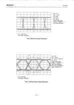
Single-phase input Fig. 8. Electrical Output Waveform Single-phase input Fig. 9. Optical Power Output Waveform
Open the catalog to page 16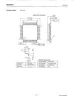
Package Outline Unit: mm PACKAGE STRUCTURE Sony Corporation
Open the catalog to page 17All Sony Semiconductors catalogs and technical brochures
 IMX901-AMR
2 Pages
 IMX490
2 Pages
 IMX290NQV
2 Pages
 ISX016
2 Pages
 IMX390CQV
2 Pages
Archived catalogs
 SLD344YT
6 Pages
 SLD432S
5 Pages
 CXA3314ER
16 Pages
 ICX205AK
24 Pages
 CXA2096N
17 Pages
 SLD433S4
5 Pages
 CXA4416GC
21 Pages
 CXA2984GC SP4T ANT SW
11 Pages
 SLD335YT
5 Pages
 CXM3807K
24 Pages
 CXM3648UR
11 Pages
 CXM3645ER
12 Pages
 CXM3642K
29 Pages
 CXM3641ER
22 Pages
 CXM3632ER
22 Pages
 CXM3630UR
15 Pages
 CXM3617ER
23 Pages
 CXM3614ER
14 Pages
 CXM3604UR
14 Pages
 CXM3599UR
15 Pages
 CXM3593UR
11 Pages
 SLD1332V
5 Pages
 CXM3592AUR
15 Pages
 CXM3583AUR
17 Pages
 CXM3582UR
17 Pages
 CXM3580UR
13 Pages
 CXM3580AUR
17 Pages
 CXM3572ER
14 Pages
 CXM3570ER
13 Pages
 CXM3569XR
13 Pages
 ICX418ALB
20 Pages
 CXD4728R
68 Pages
 ICX642BKA
23 Pages
 CXA3791EN
13 Pages
 SLD332F
6 Pages
 CXG1407XR
11 Pages
 IMX291LQR
2 Pages
 IMX252LLR/LQR
2 Pages
 IMX230
2 Pages
 IMX377CQT
5 Pages
 IMX249LLJ/LQJ
2 Pages
 IMX323LQN
2 Pages
 IMX258
2 Pages
 IMX302LQJ
2 Pages
 CXD4017R
34 Pages
 CXA3197R
30 Pages
 IMX222LQJ
2 Pages
 IMX324
2 Pages
 IMX367LLA
2 Pages
 IMX412-AACK
2 Pages
 IMX385LQR
2 Pages
 IMX294CJK
2 Pages
 IMX253LLR/LQR
2 Pages
 IMX273LLR/LQR
2 Pages
 IMX183CLK-J/CQJ-J
2 Pages
 IMX249LLJ/IMX249LQJ
2 Pages
 IMX250LLR/LQR,IMX252LLR/LQR
2 Pages
 B/W Video Camera CCD ICX422AL
17 Pages
 B/W Video Camera CCD ICX279AL*2
18 Pages
 Color Video Camera CCD ICX239AKE
18 Pages
 Color Video Camera CCD ICX418AKL
22 Pages


- Display module
- LCD display panel
- Color display panel
- LED display panel
- RGB display panel
- Compact display panel
- GNSS receiver
- Compact receiver
- Industrial receiver
- OLED display
- High-definition display module
- Satellite receiver
- Sony CMOS image sensor
- Vision sensor
- Communication card
- Full HD display
- Codec
- Fiber laser diode
- Sony visible image sensor