- Catalogs
- ON Semiconductor
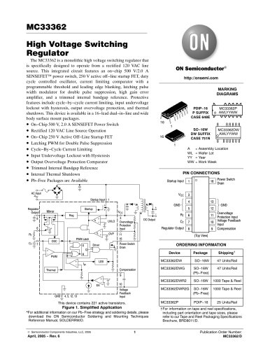
- Off-Line Regulators Current Mode Switching Regulators - Voltage Mode Switching Regulators MC33362DWG
Off-Line Regulators Current Mode Switching Regulators - Voltage Mode Switching Regulators MC33362DWG
1 /14Pages
Off-Line Regulators Current Mode Switching Regulators - Voltage Mode Switching Regulators MC33362DWG
1 /14Pages
Catalog excerpts

V > CC = 20 VA V > CC = 20 VA > V = −1.0C > V = −1.0C 1.80 V > L = 10 pFT > L = 10 pFT > A = 25 C > A = 25 а C1.75 V1.70 V 3.00 V1.75 V 0.50 V > 0.5 V/DIV 20 mV/DIV 1.0 s/DIV 1.0 s/DIV > V V = 50 VT > CC = 20 VR > pin1 T = 10 kC > A = 25 C ТȒ20−40 −60 −804.08.0121620 > PIN 8 = 1.0 FT > A = 25 C > , STARTUP CURRENT (mA) I start I Vreg, REGULATOR VOLTAGE CHANGE (mV) ТȆ 012345678 0246810121416 0 0 I > reg , REGULATOR SOURCE CURRENT (mA) V > CC , POWER SUPPLY VOLTAGE (V) > T > A = 25 C V > CC = 0 V V > CC = 14 V > , STARTUP CURRENT (mA) start 012345678 01020304050 V > pin1 , STARTUP PIN VOLTAGE (V)...
Open the catalog to page 5
Mirror VCC 3Startup Input 450 Output 2.25 II 9.0RSQDriver ProtectionInputDrain Feedback Input TT 4 I OscillatorPWMPWM Latch Current Limit ThermalShutdownError StartupControlBand GapRegulatorUVLO14.5 V/9.5 VOVP2.6 V Current 2.6 V Regulator Output6.5 VRC867 4, 5, 12, 13Gnd 1116 910 1 Voltage Compensation Power SwitchOvervoltage AC InputDC Comparator Leading Edge Blanking Comparator 270 A Amplifier > Capacitor CCompensationPWMComparatorOutputOscillator OutputPWM LatchQ Output T t Propagation Delay Power SwitchGate Drive Leading EdgeBlanking Input(Power SwitchDrain Current) CurrentLimitThreshold...
Open the catalog to page 8
The Power Switch is designed to directly drive the convertertransformer and is capable of switching a maximum of 500 V and 2.0 A. Proper device voltage snubbing andheatsinking are required for reliable operation. A Leading Edge Blanking circuit was placed in thecurrent sensing signal path. This circuit prevents apremature reset of the PWM Latch. The premature reset is generated each time the Power Switch is driven intoconduction. It appears as a narrow voltage spike across thecurrent sense resistor, and is due to the MOSFET gate to source capacitance, transformer interwinding capacitance,and...
Open the catalog to page 10
Test Conditions Results Line Regulation V > in = 92 Vac to 138 Vac, I > O 4.0 A = 1.0 mV Load Regulation V > in = 115 Vac, I > O = 1.0 A to 4.0 A = 9.0 mV Output Ripple V > in = 115 Vac, I > O = 4.0 A Triangular = 10 mVppSpike = 60 mVpp Efficiency V > in = 115 Vac, I > O = 4.0 A 78.4% This data was taken with the components listed below mounted on the printed circuit board shown in Figure 23. For high efficiency and small circuit board size, the Sanyo OsCon capacitors are recommended for C8, C9, C10 and C11.C8, C9, C10 = Sanyo OsCon #6SA330M, 330 F 6.3 V.C11 = Sanyo OsCon #10SA220M, 220 F 10...
Open the catalog to page 11
NOTES:1.DIMENSIONING AND TOLERANCING PER ANSIY14.5M, 1982.2.CONTROLLING DIMENSION: INCH. 3.DIMENSION L TO CENTER OF LEADS WHENFORMED PARALLEL.4.DIMENSION A AND B DOES NOT INCLUDE MOLDPROTRUSION.5.MOLD FLASH OR PROTRUSIONS SHALL NOTEXCEED 0.25 (0.010).6.ROUNDED CORNER OPTIONAL. 16918 > 16981 NOTES:1.DIMENSIONING AND TOLERANCING PER ANSIY14.5M, 1982.2.CONTROLLING DIMENSION: MILLIMETER. 3.DIMENSIONS A AND B DO NOT INCLUDE MOLDPROTRUSION.4.MAXIMUM MOLD PROTRUSION 0.15 (0.006) PERSIDE.5.DIMENSION D DOES NOT INCLUDE DAMBARPROTRUSION. ALLOWABLE DAMBAR PROTRUSION SHALL BE 0.13 (0.005) TOTAL INEXCESS...
Open the catalog to page 13All ON Semiconductor catalogs and technical brochures
 NCV-RSL 15
1 Page
 Networking & Telecom Solutions
28 Pages
 Smart Grid Solutions 2014
16 Pages
 LED Lighting Solutions
48 Pages
 Automotive Products Selector
36 Pages
 White Goods Solutions
32 Pages
 Smart Grid Solutions 2012
12 Pages
 Portable Solutions
28 Pages
 Networking Solutions
24 Pages
 Medical Solutions
16 Pages
 Industrial Solutions
40 Pages
 Image Sensors
12 Pages
 Home Entertainment Solutions
40 Pages
 Computing Solutions
12 Pages
 Automotive Solutions
48 Pages
 1 A Dual H
9 Pages
 Dual 2-Bit Adder / Subtractor
5 Pages
 Quad Analog Switch/Quad Multiplexer
11 Pages


Archived catalogs
 Switching Controllers
20 Pages
 High Power Audio transistors
5 Pages


- Transceiver module
- Electronic filter
- Motor controller
- Diode
- Potentiometer
- Transistor module
- Stepper motor controller
- Crystal oscillator
- Rectifier diode
- Radio transceiver module
- Electronic amplifier
- EMI filter
- SMT diode
- Band-pass electronic filter
- Bipolar transistor
- Active electronic filter
- Digital motor controller
- Surface-mount oscillator
- Light sensor
- DC drive