- Catalogs
- New Wave Research
- The EzLaze 3 Laser Cutting System
The EzLaze 3 Laser Cutting System
1 /2Pages

The EzLaze 3 Laser Cutting System
1 /2Pages
Catalog excerpts
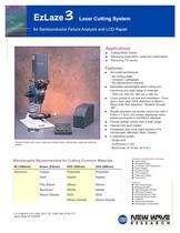
EzLaze 3 shown with power supply and remote control. Microscope, stage and stand are options. > Standard Configuration includes Laser Head Standard Energy > XY Shutter (Std. Resolution) Power Supply > Remote Control 2.4m umbilical > Video spot marker Foot switch Options High Pulse Energy Rotating Shutter > High Resolution Shutter Motorized Polarizer > Horizontal Mount Laser Head with Robot-length > Umbilical Internal Spot Marker > 2 Microscope & Accessories >
Open the catalog to page 1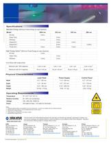
(Minimum Pulse Energy at Laser Aperture) > 4 (Minimum Pulse Energy at Laser Aperture) IR Only 2.2mJ Green Only 2.2mJ IR/Green 2.2mJ 2.2mJ Cut Size (with single pulse) Minimum with 100X objective 2 m x 2 յm 1 m x 1 յm 1 m 1 յm 2 m x 2 յm > 5 Maximum with 50 X objective 50 m x 50 յm 40 m x 40 յm 30 m x 30 յm 30 m x 30 յm > Temperature 70 10Ѱ F (21 б5 C) Relative Humidity 20З80% non-condensing Voltage 100240 VAC, 50/60 Hz Power 100 watts for laser, 215 watts for illuminator > Notes: 1. Optional rotating shutter not available for A-zoom microscope. It is also not available with the motorize polarizer....
Open the catalog to page 2All New Wave Research catalogs and technical brochures
 Nd:YAG Laser Ablation system
2 Pages
 Solo PIV
2 Pages
 UP193-FX
4 Pages
 Tempest
2 Pages
 LaserMill
2 Pages
 New Wave™
2 Pages
 UP-213 deep UV YAG
4 Pages
 MicroMill
2 Pages
 QuikLaze 50ST2
2 Pages
- Cutting system
- CNC cutting center
- Laser cutting machine
- Plastic cutting machine
- Pulsed laser
- Solid-state laser
- Fiber optic laser
- Rework station
- Infrared laser
- Nd:YAG laser
- Green laser
- Solids sampler
- Wafer cutting machine
- Laser ablation system
- Laser trimming machine
- LCD rework station
- Printed circuit laser trimming machine