
Catalog excerpts

TYPICAL APPLICATION CIRCUIT Input voltage range: 2.3 V to 6.5 V Fixed and adjustable output voltage options Fixed output voltage pair options: 1.2 V/1.8 V, 1.2 V/3.3 V, 1.8 V/3.3 V Adjustable output voltage range: 0.8 V to 6 V Minimum guaranteed continuous output current: 800 mA Up to 94% efficiency Low quiescent current of 15 µA for both channels in power saving mode (PSM) Low shutdown current: 0.1 μA (typical) 100% duty cycle for low dropout operation SYNC pin switching frequency options 2 MHz fixed pulse-width modulation (PWM) mode 2 MHz PSM/PWM automatic transitioning mode External clock synchronization from 1.5 MHz to 2.5 MHz Enable input with precision thresholds for each output 180° phase shifted PWM outputs for minimum VIN ripple Current-limit and thermal shutdown (TSD) protection Quick output discharge (QOD) 10-lead, 3 mm × 3 mm × 0.75 mm LFCSP package APPLICATIONS Portable and battery-powered equipment Automatic meter readers (WSN) Point of sales and transaction processing instruments Mobile phones Digital cameras and audio devices Medical instruments Medium format display tablets and pads GENERAL DESCRIPTION The ADP2230 includes two high efficiency, low quiescent current, 800 mA, step-down, dc-to-dc converters in a small, 10-lead, 3 mm × 3 mm, LFCSP package. The total solution requires only five tiny external components. When the ADP2230 is used with three 0603 capacitors and two 2 mm × 2 mm inductors, the total solution size is about 48 mm2, resulting in the smallest footprint solution to meet a variety of portable applications. The ADP2230 buck regulator uses a proprietary, high speed, current mode, constant frequency, PWM control scheme for excellent stability and transient response. The buck outputs operate out of phase to reduce the input current ripple. To ensure the longest battery life in portable applications, the ADP2230 has a power saving variable frequency mode that reduces the switching frequency under light load conditions. PGND (EPAD) Data Sheet Dual 2 MHz, 800 mA, Synchronous, Low Quiescent Current Buck Regulator ADP2230 Figure 1. Fixed Output Voltage Typical Application Circuit During logic controlled shutdown, the input is disconnected from the output, and it draws less than 0.1 μA from the input source. The ADP2230 operates from input voltages from 2.3 V to 6.5 V, allowing the use of multiple alkaline, NiMH, or lithium cells and other standard power sources. The ADP2230 offers multiple options for setting the operating frequency. To maximize light load efficiency, the ADP2230 can operate at a reduced switching frequency in PSM and switch automatically to PWM as the load increases. The ADP2230 can be forced to operate at 2 MHz in PWM only mode when noise considerations are more important than efficiency. The ADP2230 can also be synchronized with a 1.5 MHz to 2.5 MHz external clock via the SYNC pin. When using the external clock synchronization control, both buck outputs operate in phase with the applied clock signal. The ADP2230 includes an internal power switch, synchronous rectifier, and compensation to minimize external part count and maximize efficiency. Other key protection features include undervoltage lockout to prevent deep battery discharge, internal soft start to prevent input current overshoot at startup, and an integrated, switched resistor, QOD function that automatically discharges the output when the device is disabled. Short-circuit protection and thermal overload protection circuits prevent damage in adverse conditions. Document Feedback Information furnished by Analog Devices is believed to be accurate and reliable. However, no responsibility is assumed by Analog Devices for its use, nor for any infringements of patents or other rights of third parties that may result from its use. Specifications subject to change without notice. No license is granted by implication or otherwise under any patent or patent rights of Analog Devices. Trademarks and registered trademarks are the property of their respective owners. One Technology Way, P.O. Box 9106, Norwood, MA 02062-9106, U.S.A. Tel: 781.329.4700 ©2014 Analog Devices, Inc. All rights reserved. Technical Support www.analog.com
Open the catalog to page 1
Data Sheet REVISION HISTORY 10/14—Revision 0: Initial Version
Open the catalog to page 2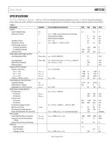
Data Sheet SPECIFICATIONS VIN = VENx = 5.0 V, VOUT = 3.3 V, TJ = −40°C to +125°C for minimum/maximum specifications, and TA = 25°C for typical specifications, unless otherwise noted. All limits at temperature extremes are guaranteed via correlation using standard statistical quality control (SQC). Table 1. Parameter SUPPLY Input Voltage Range Quiescent Current Standby Current Shutdown Current Undervoltage Lockout VIN Rising Threshold VIN Falling Threshold Soft Start Time FIXED AND ADJUSTABLE OUTPUT Load Regulation PWM Line Regulation PSM Rising Threshold PSM Hysteresis FIXED OUTPUT VOLTAGE...
Open the catalog to page 3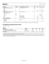
ADP2230 Parameter ENABLE STANDBY LOGIC LEVELS High Low Hysteresis ENABLE PRECISION LOGIC LEVELS Operating Maximum EN1 EN2 High Low ENx Pin Leakage Current THERMAL SHUTDOWN Threshold Hysteresis 1 Data Sheet Symbol 1.15 200 2.3 V ≤ VIN ≤ 6.5 V VEN1 VEN2 ENx pin rising ENx pin falling VENx = VIN or GND The fixed VOUT feedback pin current is the internal feedback voltage, 0.8 V (typical), divided by the bottom feedback resistor, typically 400 kΩ. RECOMMENDED COMPONENT SPECIFICATIONS TA = −40°C to +125°C Table 2. Parameter INPUT AND OUTPUT CAPACITANCE2 Capacitor Equivalent Series Resistance...
Open the catalog to page 4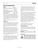
Data Sheet ABSOLUTE MAXIMUM RATINGS The specified values of θJA are based on a 4-layer, 4 in. × 3 in. circuit board. See JEDEC JESD51-7, High Effective Thermal Conductivity Test Board for Leaded Surface Mount Packages, for detailed information on board construction. For more information, see AN-772 Application Note, A Design and Manufacturing Guide for the Lead Frame Chip Scale Package (LFCSP). Table 3. Parameter VINx, FBx, EN2, SYNC to AGND, PGND EN1 SWx to AGND, PGND Operating Ambient Temperature Range Operating Junction Temperature Range Storage Temperature Range Soldering Conditions...
Open the catalog to page 5All Analog Devices catalogs and technical brochures
-
 Powering ADI Components
8 Pages
-
 HMC722LP3E
10 Pages
-
 HMC853 Data Sheet
10 Pages
-
 AN-1084
8 Pages
-
 AN-1091
2 Pages
-
 AN_737
8 Pages
-
 AN-0982
4 Pages
-
 ADF7024
24 Pages
-
 AD9915
48 Pages
-
 AD9914
48 Pages
-
 ADRF6612
59 Pages
-
 ADRF6820
48 Pages
-
 ADL5246
32 Pages
-
 ADA4961
22 Pages
-
 AN-1141
8 Pages
-
 AN-698
36 Pages
-
 Temperature Sensors
2 Pages
-
 Reference Circuits
8 Pages
-
 Precision ADCs
16 Pages
-
 ADR02ACHIPS: ADR02ACHIPS
8 Pages
-
 AD9364 RF Agile Transceiver
32 Pages
-
 Digital Temperature Sensors
2 Pages
-
 Digital to Analog Converter ICs
12 Pages
-
 AD1836A: Multichannel 96 kHz Codec
24 Pages
-
 Zero-Drift Amplifiers
2 Pages


