- Catalogs
- Analog Devices
- ADN2525: 10.7 Gbps Active Back-Termination, Differential Laser Diode Driver
- Products
- Catalogs
- News & Trends
- Exhibitions
ADN2525: 10.7 Gbps Active Back-Termination, Differential Laser Diode Driver
1 /16Pages

ADN2525: 10.7 Gbps Active Back-Termination, Differential Laser Diode Driver
1 /16Pages
Catalog excerpts
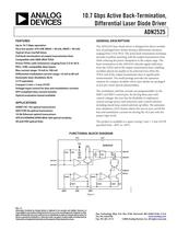
10.7 Gbps Active Back-Termination, Differential Laser Diode Driver ADN2525 Rev. A Information furnished by Analog Devices is believed to be accurate and reliable. However, no responsibility is assumed by Analog Devices for its use, nor for any infringements of patents or other rights of third parties that may result from its use. Specifications subject to change without notice. No license is granted by implication or otherwise under any patent or patent rights of Analog Devices. Trademarks and registered trademarks are the property of their respective owners. One Technology Way, P.O. Box 9106, Norwood, MA 02062-9106, U.S.A. Tel: 781.329.4700 www.analog.com Fax: 781.461.3113 ©2006 Analog Devices, Inc. All rights reserved. FEATURES Up to 10.7 Gbps operation Very low power: 670 mW (IBIAS = 40 mA, IMOD = 40 mA) Typical 24 ps rise/fall times Full back-termination of output transmission lines Compatible with XMD-MSA TOSA Drives TOSAs with resistances ranging from 5 Ù to 50 Ù PECL-/CML-compatible data inputs Bias current range: 10 mA to 100 mA Differential modulation current range: 10 mA to 80 mA Automatic laser shutdown (ALS) 3.3 V operation Compact 3 mm × 3 mm LFCSP Voltage input control for bias and modulation currents XFP-compliant bias current monitor Optical evaluation board available APPLICATIONS SONET OC-192 optical transceivers SDH STM-64 optical transceivers 10 Gb Ethernet optical transceivers XFP/X2/XENPAK/XPAK/MSA 300 optical modules SR and VSR optical links GENERAL DESCRIPTION The ADN2525 laser diode driver is designed for direct modula-tion of packaged laser diodes having a differential resistance ranging from 5 Ù to 50 Ù. The active back-termination technique provides excellent matching with the output transmission lines while reducing the power dissipation in the output stage. The back-termination in the ADN2525 absorbs signal reflections from the TOSA end of the output transmission lines, enabling excellent optical eye quality to be achieved even when the TOSA end of the output transmission lines is significantly misterminated. The small package provides the optimum solution for compact modules where laser diodes are packaged in low pin-count optical subassemblies. The modulation and bias currents are programmable via the MSET and BSET control pins. By driving these pins with control voltages, the user has the flexibility to implement various average power and extinction ratio control schemes, including closed-loop control and look-up tables. The automatic laser shutdown (ALS) feature allows the user to turn on/off the bias and modulation currents by driving the ALS pin with the proper logic levels. The product is available in a space-saving 3 mm × 3 mm LFCSP specified from -40°C to +85°C. FUNCTIONAL BLOCK DIAGRAM 50Ù200Ù800Ù200Ù2ÙVCCDATAPDATANMSETGNDBSETIBMONIBIASIMODPIMODNADN2525VCCALSGNDVCCVCC50Ù50Ù200Ù800ÙIMOD05077-001 Figure 1.
Open the catalog to page 1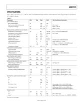
ADN2525 Rev. A | Page 3 of 16 SPECIFICATIONS VCC = VCCMIN to VCCMAX, TA = -40°C to +85°C, 50 Ù differential load resistance, unless otherwise noted. Typical values are specified at 25°C, IMOD = 40 mA. Table 1. Parameter Min Typ Max Unit Test Conditions/Comments BIAS CURRENT (IBIAS) Bias Current Range 10 100 mA Bias Current while ALS Asserted 100 ìA ALS = high Compliance Voltage1 0.6 VCC – 1.2 V IBIAS = 100 mA 0.6 VCC – 0.8 V IBIAS = 10 mA MODULATION CURRENT (IMODP, IMODN) Modulation Current Range 10 80 mA diff RLOAD = 5 Ù to 50 Ù differential Modulation Current While ALS Asserted 0.5 mA diff...
Open the catalog to page 3
ADN2525 Rev. A | Page 4 of 16 1 Refers to the voltage between the pin for which the compliance voltage is specified and GND. 2 The pattern used is composed by a repetitive sequence of eight 1s followed by eight 0s at 10.7 Gbps. 3 Measured using the high speed characterization circuit shown in Figure 3. 4 The pattern used is K28.5 (00111110101100000101) at a 10.7 Gbps rate. 5 Only includes current in the ADN2525 VCC pins. 6 Includes current in ADN2525 VCC pins and dc current in IMODP and IMODN pull-up inductors. See the Power Consumption section for total supply current calculation. THERMAL SPECIFICATIONS...
Open the catalog to page 4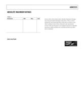
ADN2525 Rev. A | Page 5 of 16 ABSOLUTE MAXIMUM RATINGS Table 3. Parameter Min Max Unit Supply Voltage, VCC to GND -0.3 +4.2 V IMODP, IMODN to GND VCC - 1 .5 4.75 V DATAP, DATAN to GND VCC - 1.8 VCC - 0.4 V All Other Pins -0.3 VCC + 0.3 V Junction Temperature 150 °C Storage Temperature Range -65 +150 °C Soldering Temperature (Less than 10 sec) 300 °C Stresses above those listed under Absolute Maximum Ratings may cause permanent damage to the device. This is a stress rating only; functional operation of the device at these or any other conditions above those indicated in the operational section...
Open the catalog to page 5
ADN2525 Rev. A | Page 6 of 16 PIN CONFIGURATION AND FUNCTION DESCRIPTIONS NC = NO CONNECT1211109GNDIBIASIBMONBSET1MSET235VCCIMODNIMODPVCC6784GNDALSNC16151413ADN2525TOP VIEW(Not to ScalePIN 1INDICATORVCCDATANDATAPVCC05077-016 Figure 4. Pin Configuration Note that the exposed pad on the bottom of the package must be connected to the VCC or GND plane. Table 4. Pin Function Description Pin No. Mnemonic I/O Description 1 MSET Input Modulation Current Control Input 2 NC N/A No Connect—Leave Floating 3 ALS Input Automatic Laser Shutdown 4 GND Power Negative Power Supply 5 VCC Power Positive Power Supply...
Open the catalog to page 6
ADN2525 Rev. A | Page 7 of 16 TYPICAL PERFORMANCE CHARACTERISTICS TA = 25°C, VCC = 3.3 V, unless otherwise noted. DIFFERENTIAL MODULATION CURRENT (mA)100020406080RISE TIME ( ps)28.023.524.024.525.025.526.026.527.027.523.005077-004 Figure 5. Rise Time vs. IMOD DIFFERENTIAL MODULATION CURRENT (mA)100020406080FALL TIME ( ps)27.526.527.025.526.025.024.024.523.523.005077-005 Figure 6. Fall Time vs. IMOD DIFFERENTIAL MODULATION CURRENT (mA)100020406080RANDOM JITTER ( ps rms)0.70.50.60.40.30.20.1005077-006 Figure 7. Random Jitter vs. IMOD DIFFERENTIAL MODULATION CURRENT (mA)100020406080DETERMINISTIC...
Open the catalog to page 7All Analog Devices catalogs and technical brochures
 HMC722LP3E
8 Pages
 Isolated Sigma-Delta Modulator
17 Pages
 HMC853 Data Sheet
10 Pages
 AN-1084
8 Pages
 AN-1091
2 Pages
 AN_737
8 Pages
 AN-0982
4 Pages
 ADF7024
24 Pages
 AD9915
48 Pages
 AD9914
48 Pages
 ADRF6612
59 Pages
 ADRF6820
48 Pages
 ADL5246
32 Pages
 ADA4961
22 Pages
 AN-1141
8 Pages
 AN-698
36 Pages
 Temperature Sensors
2 Pages
 Reference Circuits
8 Pages
 Precision ADCs
16 Pages
 ADR02ACHIPS: ADR02ACHIPS
8 Pages
 AD9364 RF Agile Transceiver
32 Pages
 Digital Temperature Sensors
2 Pages
 Digital to Analog Converter ICs
12 Pages
 AD1836A: Multichannel 96 kHz Codec
24 Pages


Archived catalogs
 Zero-Drift Amplifiers
2 Pages
 Powering ADI Components
8 Pages


- Ethernet switch
- Industrial network switch
- Acceleration sensor
- Unmanaged switch
- Analog Devices motor controller
- Triaxial acceleration sensor
- DC motor controller
- Data acquisition unit
- Analog Devices stepper motor controller
- Industrial converter
- Ethernet transceiver
- Processor
- Multiplexer
- High-voltage amplifier
- Low-noise amplifier
- Compact motor controller
- Digital converter
- Gyroscope
- Closed-loop motor controller