- Catalogs
- Analog Devices
- AD5337: 2.5 V to 5.5 V, 250 µA, 2-Wire Interface, Dual Voltage Output, 8-Bit DACs
- Products
- Catalogs
- News & Trends
- Exhibitions
AD5337: 2.5 V to 5.5 V, 250 µA, 2-Wire Interface, Dual Voltage Output, 8-Bit DACs
1 /28Pages

AD5337: 2.5 V to 5.5 V, 250 µA, 2-Wire Interface, Dual Voltage Output, 8-Bit DACs
1 /28Pages
Catalog excerpts
2.5 V to 5.5 V, 250 ìA, 2-Wire Interface, Dual Voltage Output, 8-/10-/12-Bit DACs AD5337/AD5338/AD5339 Rev. C Information furnished by Analog Devices is believed to be accurate and reliable. However, no responsibility is assumed by Analog Devices for its use, nor for any infringements of patents or other rights of third parties that may result from its use. Specifications subject to change without notice. No license is granted by implication or otherwise under any patent or patent rights of Analog Devices. Trademarks and registered trademarks are the property of their respective owners. One Technology Way, P.O. Box 9106, Norwood, MA 02062-9106, U.S.A. Tel: 781.329.4700 www.analog.com Fax: 781.461.3113 ©2003–2007 Analog Devices, Inc. All rights reserved. FEATURES AD5337 2 buffered 8-bit DACs in 8-lead MSOP AD5338, AD5338-1 2 buffered 10-bit DACs in 8-lead MSOP AD5339 2 buffered 12-bit DACs in 8-lead MSOP Low power operation: 250 ìA @ 3 V, 300 ìA @ 5 V 2-wire (I2C-compatible) serial interface 2.5 V to 5.5 V power supply Guaranteed monotonic by design over all codes Power-down to 80 nA @ 3 V, 200 nA @ 5 V 3 power-down modes Double-buffered input logic Output range: 0 V to VREF Power-on reset to 0 V Simultaneous update of outputs (LDAC function) Software clear facility Data readback facility On-chip rail-to-rail output buffer amplifiers Temperature range: -40°C to +105°C APPLICATIONS Portable battery-powered instruments Digital gain and offset adjustment Programmable voltage and current sources Programmable attenuators Industrial process control GENERAL DESCRIPTION The AD5337/AD5338/AD5339 are dual 8-, 10-, and 12-bit buffered voltage output DACs, respectively. Each part is housed in an 8-lead MSOP package and operates from a single 2.5 V to 5.5 V supply, consuming 250 ìA at 3 V. On-chip output amplifiers allow rail-to-rail output swing with a slew rate of 0.7 V/ìs. A 2-wire serial interface operates at clock rates up to 400 kHz. This interface is SMBus compatible at VDD < 3.6 V. Multiple devices can be placed on the same bus. The references for the two DACs are derived from one reference pin. The outputs of all DACs can be updated simultaneously using the software LDAC function. The parts incorporate a power-on reset circuit to ensure that the DAC outputs power up to 0 V and remain there until a valid write to the device takes place. A software clear function resets all input and DAC registers to 0 V. A power-down feature reduces the current consumption of the devices to 200 nA @ 5 V (80 nA @ 3 V). The low power consumption of these parts in normal operation makes them ideally suited to portable battery-operated equip-ment. The power consumption is typically 1.5 mW at 5 V and 0.75 mW at 3 V, reducing to 1 ìW in power-down mode. FUNCTIONAL BLOCK DIAGRAM SCLBUFFERBUFFERLDACA0SDAGND03756-001INTERFACELOGICINPUTREGISTERINPUTREGISTERDACREGISTERDACREGISTERSTRINGDACASTRINGDACBVOUTAVOUTBPOWER-DOWNLOGICAD5337/AD5338/AD5339POWER-ONRESETREFINVDD Figure 1.
Open the catalog to page 1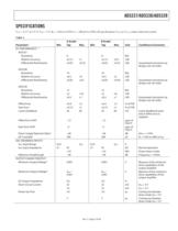
AD5337/AD5338/AD5339 Rev. C | Page 3 of 28 SPECIFICATIONS VDD = 2.5 V to 5.5 V; VREF = 2 V; RL = 2 kÙ to GND; CL = 200 pF to GND; all specifications TMIN to TMAX, unless otherwise noted. Table 1. A Grade1 B Grade1 Parameter2 Min Typ Max Min Typ Max Unit Conditions/Comments DC PERFORMANCE3, 4 AD5337 Resolution 8 8 Bits Relative Accuracy ±0.15 ±1 ±0.15 ±0.5 LSB Differential Nonlinearity ±0.02 ±0.25 ±0.02 ±0.25 LSB Guaranteed monotonic by design over all codes AD5338 Resolution 10 10 Bits Relative Accuracy ±0.5 ±4 ±0.5 ±2 LSB Differential Nonlinearity ±0.05 ±0.5 ±0.05 ±0.50 LSB Guaranteed monotonic...
Open the catalog to page 3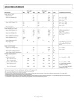
AD5337/AD5338/AD5339 Rev. C | Page 4 of 28 A Grade1 B Grade1 LOGIC INPUTS (A0)5 Input Current ±1 ±1 ìA Input Low Voltage (VIL) 0.8 0.8 V VDD = 5 V ± 10% 0.6 0.6 V VDD = 3 V ± 10% 0.5 0.5 V VDD = 2.5 V Input High Voltage (VIH) 2.4 2.4 V VDD = 5 V ± 10% 2.1 2.1 V VDD = 3 V ± 10% 2.0 2.0 V VDD = 2.5 V Pin Capacitance 3 3 pF LOGIC INPUTS (SCL, SDA)5 Input High Voltage (VIH) 0.7 × VDD VDD + 0.3 0.7 × VDD VDD + 0.3 V SMBus compatible at VDD < 3.6 V Input Low Voltage (VIL) -0.3 +0.3 VDD –0.3 +0.3 VDD V SMBus compatible at VDD < 3.6 V Input Leakage Current (IIN) ±1 ±1 ìA Input Hysteresis (VHYST) 0.05...
Open the catalog to page 4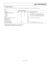
AD5337/AD5338/AD5339 Rev. C | Page 5 of 28 AC CHARACTERISTICS VDD = 2.5 V to 5.5 V; RL = 2 kÙ to GND; CL = 200 pF to GND; all specifications TMIN to TMAX, unless otherwise noted. Table 2. A Version and B Version1 Parameter2, 3 Min Typ Max Unit Conditions/Comments Output Voltage Settling Time VREF = VDD = 5 V AD5337 6 8 ìs 1/4 scale to 3/4 scale change (0x40 to 0xC0) AD5338 7 9 ìs 1/4 scale to 3/4 scale change (0x100 to 0x300) AD5339 8 10 ìs 1/4 scale to 3/4 scale change (0x400 to 0xC00) Slew Rate 0.7 V/ìs Major Code Transition Glitch Energy 12 nV-s 1 LSB change around major carry Digital Feedthrough...
Open the catalog to page 5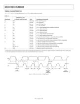
AD5337/AD5338/AD5339 Rev. C | Page 6 of 28 TIMING CHARACTERISTICS VDD = 2.5 V to 5.5 V. All specifications TMIN to TMAX, unless otherwise noted. Table 3. Limit at TMIN, TMAX Parameter A Version and B Version Unit Conditions/Comments fSCL 400 kHz max SCL clock frequency t1 2.5 ìs min SCL cycle time t2 0.6 ìs min tHIGH, SCL high time t3 1.3 ìs min tLOW, SCL low time t4 0.6 ìs min tHD, STA, start/repeated start condition hold time t5 100 ns min tSU, DAT, data setup time t61 0.9 ìs max tHD, DAT, data hold time 0 ìs min tHD, DAT, data hold time t7 0.6 ìs min tSU, STA, setup time for repeated start...
Open the catalog to page 6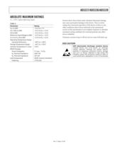
AD5337/AD5338/AD5339 Rev. C | Page 7 of 28 ABSOLUTE MAXIMUM RATINGS TA = 25°C, unless otherwise noted. Table 4. Parameter Rating VDD to GND -0.3 V to +7 V SCL, SDA to GND -0.3 V to VDD + 0.3 V A0 to GND -0.3 V to VDD + 0.3 V Reference Input Voltage to GND -0.3 V to VDD + 0.3 V VOUTA to VOUTB to GND -0.3 V to VDD + 0.3 V Operating Temperature Range Industrial (B Version) -40°C to +105°C Storage Temperature Range -65°C to +150°C Junction Temperature (TJ max) 150°C MSOP Package Power Dissipation (TJ max - TA) èJA èJA Thermal Impedance 206°C/W èJC Thermal Impedance 44°C/W Lead Temperature JEDEC Industry...
Open the catalog to page 7All Analog Devices catalogs and technical brochures
 HMC722LP3E
8 Pages
 Isolated Sigma-Delta Modulator
17 Pages
 HMC853 Data Sheet
10 Pages
 AN-1084
8 Pages
 AN-1091
2 Pages
 AN_737
8 Pages
 AN-0982
4 Pages
 ADF7024
24 Pages
 AD9915
48 Pages
 AD9914
48 Pages
 ADRF6612
59 Pages
 ADRF6820
48 Pages
 ADL5246
32 Pages
 ADA4961
22 Pages
 AN-1141
8 Pages
 AN-698
36 Pages
 Temperature Sensors
2 Pages
 Reference Circuits
8 Pages
 Precision ADCs
16 Pages
 ADR02ACHIPS: ADR02ACHIPS
8 Pages
 AD9364 RF Agile Transceiver
32 Pages
 Digital Temperature Sensors
2 Pages
 Digital to Analog Converter ICs
12 Pages
 AD1836A: Multichannel 96 kHz Codec
24 Pages


Archived catalogs
 Zero-Drift Amplifiers
2 Pages
 Powering ADI Components
8 Pages


- Ethernet switch
- Industrial network switch
- Acceleration sensor
- Unmanaged switch
- Transceiver module
- Analog Devices motor controller
- Triaxial acceleration sensor
- DC motor controller
- Data acquisition unit
- Analog Devices stepper motor controller
- Industrial converter
- Ethernet transceiver
- Processor
- Low-noise amplifier
- High-voltage amplifier
- Multiplexer
- Compact motor controller
- Digital converter
- Gyroscope
- Closed-loop motor controller